


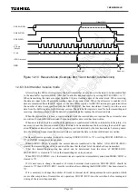
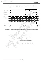
Page 132
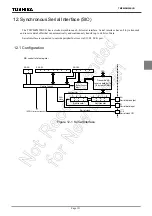
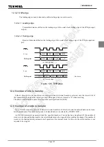
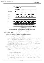
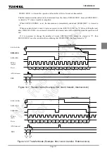
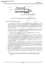
12. Synchronous Serial Interface (SIO)
12.2 Control
TMP86PM29BUG
12.2 Control
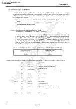
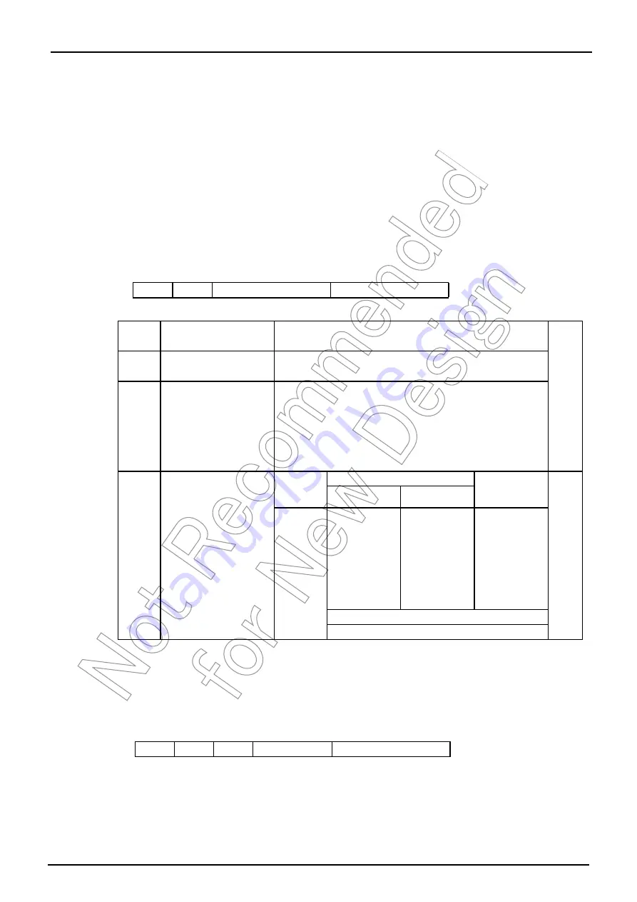
The serial interface is controlled by SIO control registers (SIOCR1/SIOCR2). The serial interface status can be
determined by reading SIO status register (SIOSR).
The transmit and receive data buffer is controlled by the SIOCR2<BUF>. The data buffer is assigned to address
0F90H to 0F97H for SIO in the DBR area, and can continuously transfer up to 8 words (bytes or nibbles) at one time.
When the specified number of words has been transferred, a buffer empty (in the transmit mode) or a buffer full (in
the receive mode or transmit/receive mode) interrupt (INTSIO) is generated.
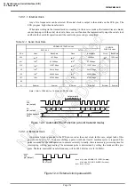
When the internal clock is used as the serial clock in the 8-bit receive mode and the 8-bit transmit/receive mode, a
fixed interval wait can be applied to the serial clock for each word transferred. Four different wait times can be
selected with SIOCR2<WAIT>.
Note 1: fc; High-frequency clock [Hz], fs; Low-frequency clock [Hz]
Note 2: Set SIOS to "0" and SIOINH to "1" when setting the transfer mode or serial clock.
Note 3: SIOCR1 is write-only register, which cannot access any of in read-modify-write instruction such as bit operate, etc.
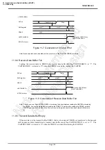
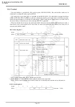
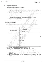
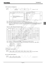
SIO Control Register 1
SIOCR1
7
6
5
4
3
2
1
0
(0F98H)
SIOS
SIOINH
SIOM
SCK
(Initial value: 0000 0000)
SIOS
Indicate transfer start / stop
0:
Stop
Write
only
1:
Start
SIOINH
Continue / abort transfer
0:
Continuously transfer
1:
Abort transfer (Automatically cleared after abort)
SIOM
Transfer mode select
000:
8-bit transmit mode
010:
4-bit transmit mode
100:
8-bit transmit / receive mode
101:
8-bit receive mode
110:
4-bit receive mode
Except the above: Reserved
SCK
Serial clock select
NORMAL1/2, IDLE1/2 mode
SLOW1/2
SLEEP1/2
mode
Write
only
DV7CK = 0
DV7CK = 1
000
fc/2
13
fs/2
5
fs/2
5
001
fc/2
8
fc/2
8
-
010
fc/2
7
fc/2
7
-
011
fc/2
6
fc/2
6
-
100
fc/2
5
fc/2
5
-
101
fc/2
4
fc/2
4
-
110
Reserved
111
External clock ( Input from SCK pin )
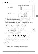
SIO Control Register 2
SIOCR2
7
6
5
4
3
2
1
0
(0F99H)
WAIT
BUF
(Initial value: ***0 0000)
Summary of Contents for TLCS-870/C Series
Page 1: ...8 Bit Microcontroller TLCS 870 C Series TMP86PM29BUG ...
Page 6: ...TMP86PM29BUG ...
Page 7: ...Revision History Date Revision 2007 10 11 1 First Release 2008 8 29 2 Contents Revised ...
Page 9: ......
Page 15: ...vi ...
Page 19: ...Page 4 1 3 Block Diagram TMP86PM29BUG 1 3 Block Diagram Figure 1 2 Block Diagram ...
Page 23: ...Page 8 1 4 Pin Names and Functions TMP86PM29BUG ...
Page 48: ...Page 33 TMP86PM29BUG ...
Page 49: ...Page 34 2 Operational Description 2 3 Reset Circuit TMP86PM29BUG ...
Page 61: ...Page 46 3 Interrupt Control Circuit 3 8 External Interrupts TMP86PM29BUG ...
Page 81: ...Page 66 6 Watchdog Timer WDT 6 3 Address Trap TMP86PM29BUG ...
Page 135: ...Page 120 10 8 Bit TimerCounter TC5 TC6 10 1 Configuration TMP86PM29BUG ...
Page 145: ...Page 130 11 Asynchronous Serial interface UART 11 9 Status Flag TMP86PM29BUG ...
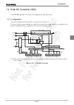
Page 165: ...Page 150 13 10 bit AD Converter ADC 13 6 Precautions about AD Converter TMP86PM29BUG ...
Page 183: ...Page 168 15 LCD Driver 15 4 Control Method of LCD Driver TMP86PM29BUG ...
Page 201: ...Page 186 18 Electrical Characteristics 18 9 Handling Precaution TMP86PM29BUG ...
Page 203: ...Page 188 19 Package Dimensions TMP86PM29BUG ...
Page 205: ......


