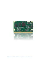
background image

SMARC T335x Carrier Board Hardware Design Guide, Document Revision 1.2


SMARC T335x Carrier Board 

Hardware Design Guide 

Summary of Contents for SMARC T335 Series

Page 1: ...SMARC T335x Carrier Board Hardware Design Guide Document Revision 1 2 SMARC T335x Carrier Board Hardware Design Guide ...

Page 2: ...SMARC T335x Carrier Board Hardware Design Guide Document Revision 1 2 ...

Page 3: ... 2 Revision History Revision Date Changes from Previous Revision 1 0 2013 7 26 Initial Release 1 2 2014 04 19 Update to Hardware rev 00B0 1 Remove the 10k pull ups on USB_EN_OC 2 Add SDIO_PWREN Schematics 3 Rename Evaluation Carrier Board from Smartbase T3 to SMART BEE ...

Page 4: ...ollowing lists the trademarks of components used in this board ARM is a registered trademark of ARM Limited Android is a registered trademark of Google Linux is a registered trademark of Linus Torvalds WinCE is a registered trademark of Microsoft TI is a registered trademark of Texas Instruments All other products and trademarks mentioned in this manual are trademarks of their respective owners St...

Page 5: ...hnicians and engineers from EMBEDIAN and or its subsidiaries and official distributors are available for technical support We are committed to making our product easy to use and will help you use our products in your systems Before contacting EMBEDIAN technical support please consult our Web site for the latest product documentation utilities and drivers If the information does not help solve the ...

Page 6: ...FACE 85 2 9 SPI INTERFACE 90 2 10 I2C BUS INTERFACE 95 2 11 SELECTING THE BOOT MODE 99 2 12 WATCHDOG CONTROL SIGNALS 101 CHAPTER 3 POWER DESIGN GUIDELINE 104 3 1 POWER SIGNALS 104 3 2 RTC BATTERY 108 3 3 POWER FLOW AND CONTROL SIGNALS BLOCK DIAGRAM 109 3 4 POWER STATES 111 3 5 POWER SEQUENCES 112 3 6 LAYOUT REQUIREMENTS 116 3 7 REFERENCE SCHEMATICS 117 CHAPTER 4 FLOOR PLANNING THE PCB 120 4 1 CARR...

Page 7: ...asis new terms variables and document titles monospaced type Filenames pathnames and code examples Embedian Information Document Updates Please always check the product specific section on the Embedian support website at www embedian com for the most current revision of this document Contact Information For more information about your Embedian products or for customer service and technical support...

Page 8: ...ardware Design Guide Document Revision 1 2 Additional Resources Please also refer to the most recent Embedian SMARC T335X user s manual or TI AM335x processor reference manual and related documentation for additional information ...

Page 9: ...re Design Guide Document Revision 1 2 Introduction This Chapter gives background information on this document Section includes Acronyms and Abbreviations Used Signal Table Terminology Document and Standard References Intended Audience ...

Page 10: ...ARC specification Therefore it is strongly recommended to read the user s manual of the SMARC T335X modules that are required to be support by the carrier board This carrier board hardware design guide for SMARC T335X computer on module helps walk hardware designers through the various stages of designing a carrier board on this platform Using this document hardware designers can efficiently locat...

Page 11: ... Serial Interface EDID Extended Display Identification Data timing setting information provided by the display in a PROM EMI Electromagnetic Interference high frequency disturbances eMMC Embedded Multi Media Card flash memory combined with MMC interface controller in a BGA package used as internal flash memory ESD Electrostatic Discharge high voltage spike or spark that can damage electrostatic se...

Page 12: ...essful application was the Flat Panel Display Link LVDS became a synonymous for this interface In this document the term LVDS is used for the Flat Panel Display Link interface MDI Medium Dependent Interface physical interface between Ethernet PHY and cable connector MDIX Medium Dependent Interface Crossed an MDI interface with crossed RX and TX interfaces MSB Most Significant Bit MXM3 Mobile PCI E...

Page 13: ... half duplex multi drop configuration possible SD Secure Digital flash memory card SDIO Secure Digital Input Output an external bus for peripherals that uses the SD interface SOC System on a Chip IC which integrates the main component of a computer on a single chip SPI Serial Peripheral Interface Bus synchronous four wire full duplex bus for peripherals TVS Diode Transient Voltage Suppression Diod...

Page 14: ...l signal can be input or output Bi Dir OD Bi directional signal output from the Module is open drain VDD_IN Signal may be exposed to Module input voltage range 3 35 to 5 25V CMOS 1 8V CMOS logic input and or output 1 8V I O supply level or tolerance CMOS 3 3V CMOS logic input and or output 3 3V I O supply level or tolerance CMOS VDD_IO CMOS logic I O level set to 3 3V for SMATC T335X Modules CMOS ...

Page 15: ...n 10 100Base TX Differential signaling using MLT 3 tri level format for 100 MBit Sec full duplex Ethernet REF Reference voltage output May be sourced from a Module power plane PDS Pull down strap A Module output pin that is either tied to GND or is not connected Used to signal Module capabilities pin out type to the Carrier Board P Power input output Schematic examples are drawn with signal direct...

Page 16: ...der the various system power states is shown in the table Term S0 On S3 Suspend to RAM S4 Suspend to Disk S5 Soft Off G3 Mechanical Off VDD_IN 3 35V 5 25 V 3 35V 5 25 V 3 35V 5 25 V 3 35V 5 25 V Off VDD_50 5V Off Off Off Off VDD_33 3 3V Off Off Off Off AUD_33 3 3V Off Off Off Off VDD_18 1 8V Off Off Off Off VDD_RTC 3 0V 3 0V 3 0V 3 0V 3 0V ...

Page 17: ...heral Interface de facto serial interface standard defined by Motorola A good description may be found on Wikipedia http en wikipedia org wiki Serial_Peripheral_Interface_Bus USB Specifications www usb org 1 3 2 SGET Documents SMARC_Hardware_Specification_V1p0 version 1 0 December 20 2012 1 3 3 Embedian Documents The following documents are listed for reference The Module schematic is not usually ...

Page 18: ... Manual April 15 2013 rev H AM335x Power Consumption Summary Oct 31 2011 1 3 5 TI Development Tools Pin Mux Utility for ARM Microprocessors Power Estimation Tool PET 1 3 6 TI Software Documents LINUXEZSDK AM335x ANDROIDDEVKIT JB AM335x 1 3 7 Embedian Software Documents Embedian Linux BSP for SMARC T335X Module Embedian Android BSP for SMARC T335X Module Embedian Linux BSP User s Guide Embedian And...

Page 19: ...x Carrier Board Hardware Design Guide Document Revision 1 2 1 4 Intended Audience This design guide is intended for electronics engineers and PCB layout engineers designing Carrier Boards for SMARC T335X Modules ...

Page 20: ...ementation guideline found on SMARC T335X connectors Section includes SMARC T335X Connector Pin Mapping Ethernet Interface USB Interface Parallel RGB LCD Interface SD SDIO Interface I2C Audio Interface CAN BUS Interface Serial COM Port Interface SPI Interface I2C BUS Interface Selecting the Boot Mode Watchdog Control Signals ...

Page 21: ...S Pin Secondary Bottom Side S1 PCAM_VSYNC P1 PCAM_PXL_CK1 S2 PCAM_HSYNC P2 GND S3 GND P3 CSI1_CK PCAM_D0 S4 PCAM_PXL_CK0 P4 CSI1_CK PCAM_D1 S5 I2C_CAM_CK P5 PCAM_DE S6 CAM_MCK P6 PCAM_MCK S7 I2C_CAM_DAT P7 CSI1_D0 PCAM_D2 S8 CSI0_CK PCAM_D10 P8 CSI1_D0 PCAM_D3 S9 CSI0_CK PCAM_D11 P9 GND S10 GND P10 CSI1_D1 PCAM_D4 S11 CSI0_D0 PCAM_D12 P11 CSI1_D1 PCAM_D5 S12 CSI0_D0 PCAM_D13 P12 GND S13 GND P13 CS...

Page 22: ...P26 GBE_MDI1 S27 SDMMC_D1 P27 GBE_MDI1 S28 SDMMC_D2 P28 GBE_CTREF S29 SDMMC_D3 P29 GBE_MDI0 S30 SDMMC_D4 P30 GBE_MDI0 S31 SDMMC_D5 P31 SPI0_CS1 S32 SDMMC_D6 P32 GND S33 SDMMC_D7 P33 SDIO_WP S34 GND P34 SDIO_CMD S35 SDMMC_CK P35 SDIO_CD S36 SDMMC_CMD P36 SDIO_CK S37 SDMMC_RST P37 SDIO_PWR_EN S38 AUDIO_MCK P38 GND S39 I2S0_LRCK P39 SDIO_D0 S40 I2S0_SDOUT P40 SDIO_D1 S41 I2S0_SDIN P41 SDIO_D2 S42 I2S...

Page 23: ... P51 SATA_RX S52 I2S2_SDIN P52 SATA_RX S53 I2S2_CK P53 GND S54 SATA_ACT P54 SPI1_CS0 S55 AFB8_PTIO P55 SPI1_CS1 S56 AFB9_PTIO P56 SPI1_CK S57 PCAM_ON_CSI0 P57 SPI1_DIN S58 PCAM_ON_CSI1 P58 SPI1_DO S59 SPDIF_OUT P59 GND S60 SPDIF_IN P60 USB0 S61 GND P61 USB0 S62 AFB_DIFF0 P62 USB0_EN_OC S63 AFB_DIFF0 P63 USB0_VBUS_DET S64 GND P64 USB0_OTG_ID S65 AFB_DIFF1 P65 USB1 S66 AFB_DIFF1 P66 USB1 S67 GND P67...

Page 24: ...RST S76 PCIE_B_RST P76 PCIE_C_CKREQ S77 PCIE_C_RST P77 PCIE_B_CKREQ S78 PCIE_C_RX P78 PCIE_A_CKREQ S79 PCIE_C_RX P79 GND S80 GND P80 PCIE_C_REFCK S81 PCIE_C_TX P81 PCIE_C_REFCK S82 PCIE_C_TX P82 GND S83 GND P83 PCIE_A_REFCK S84 PCIE_B_REFCK P84 PCIE_A_REFCK S85 PCIE_B_REFCK P85 GND S86 GND P86 PCIE_A_RX S87 PCIE_B_RX P87 PCIE_A_RX S88 PCIE_B_RX P88 GND S89 GND P89 PCIE_A_TX S90 PCIE_B_TX P90 PCIE_...

Page 25: ...HDMI_CK S103 LCD_D9 P103 GND S104 LCD_D10 P104 HDMI_HPD S105 LCD_D11 P105 HDMI_CTRL_CK S106 LCD_D12 P106 HDMI_CTRL_DAT S107 LCD_D13 P107 HDMI_CEC S108 LCD_D14 P108 GPIO0 CAM0_PWR S109 LCD_D15 P109 GPIO1 CAM1_PWR S110 GND P110 GPIO2 CAM0_RST S111 LCD_D16 P111 GPIO3 CAM1_RST S112 LCD_D17 P112 GPIO4 HDA_RST S113 LCD_D18 P113 GPIO5 PWM_OUT S114 LCD_D19 P114 GPIO6 TACHIN S115 LCD_D20 P115 GPIO7 PCAM_FL...

Page 26: ...2 S126 LVDS0 P126 RESET_OUT S127 LCD_BKLT_EN P127 RESET_IN S128 LVDS1 P128 POWER_BTN S129 LVDS1 P129 SER0_TX S130 GND P130 SER0_RX S131 LVDS2 P131 SER0_RTS S132 LVDS2 P132 SER0_CTS S133 LCD_VDD_EN P133 GND S134 LVDS_CK P134 SER1_TX S135 LVDS_CK P135 SER1_RX S136 GND P136 SER2_TX S137 LVDS3 P137 SER2_RX S138 LVDS3 P138 SER2_RTS S139 I2C_LCD_CK P139 SER2_CTS S140 I2C_LCD_DAT P140 SER3_TX S141 LCD_BK...

Page 27: ...CHARGING P151 VDD_IN S152 CHARGER_PRSNT P152 VDD_IN S153 CARRIER_STBY P153 VDD_IN S154 CARRIER_PWR_ON P154 VDD_IN S155 FORCE_RECOV P155 VDD_IN S156 BATLOW S158 VDD_IO_SEL Note The text in grey represents the signals defined in SMARC specification but not implemented in SMARC T335X The text in yellow represents the signals shared with RMII2 signals and default are configured as LAN2 function Please...

Page 28: ...SMARC T335x Carrier Board Hardware Design Guide Document Revision 1 2 Figure 2 SMARC T335X Connector Schematics I ...

Page 29: ...SMARC T335x Carrier Board Hardware Design Guide Document Revision 1 2 Figure 3 SMARC T335X Connector Schematics II ...

Page 30: ...nd pattern The schema deviates from the unrelated MXM3 standard pin numbering schema and is compliant to SMARC specification version 1 0 Pins on the primary top side of the module have a label P and pins on the secondary bottom side have a label S Pins which do not exist due to the connector notch are not accounted for pins P74 through P75 and S75 through S76 Figure 4 SMARC T335X edge finger prima...

Page 31: ...nals on SMARC MXM3 connector that is provided over the edge fingers of the SMARC module Refer to the SMARC Specification for information about this The symbol at the end of the signal name indicates that the active or asserted state occurs when the signal is at a low voltage level When is not present the signal is asserted when at a high voltage level Differential pairs are indicated by trailing a...

Page 32: ...ntial pair signals designated from GBE_MDI0 and to GBE_MDI3 and plus additional control signals for link activity indicators These signals can be used to connect a 10 100 1000BaseT RJ45 connector with integrated or external isolation magnetics to the carrier board SMARC T335X module equips with two Fast Ethernet interfaces 10 100Base TX that uses the MDI0 as transmitting lanes and the MDI1 as rece...

Page 33: ... T DB 10 100Base TX Receive P24 GBE_MDI2 IO Analogue 1000Base T DC 10 100Base TX Unused P23 GBE_MDI2 IO Analogue 1000Base T DC 10 100Base TX Unused P20 GBE_MDI3 IO Analogue 1000Base T DD 10 100Base TX Unused P19 GBE_MDI3 IO Analogue 1000Base T DD 10 100Base TX Unused P28 GBE_CTREF O Analogue Centre tap supply P25 GBE_LINK_ACK OD CMOS 3 3V LED indication output for activity on the Ethernet port P21...

Page 34: ...FB_DIFF2 GBE1_MDI2 IO Analogue 1000Base T DC 10 100Base TX Unused S69 AFB_DIFF2 GBE1_MDI2 IO Analogue 1000Base T DC 10 100Base TX Unused S71 AFB_DIFF3 GBE1_MDI3 IO Analogue 1000Base T DD 10 100Base TX Unused S72 AFB_DIFF3 GBE1_MDI3 IO Analogue 1000Base T DD 10 100Base TX Unused S17 AFB0_OUT GBE1_CTREF O Analogue Centre tap supply S55 AFB8_PTIO GBE1_LINK_ACK OD CMOS 3 3V LED indication output for a...

Page 35: ...isolation magnetics module and or improper PCB layout of the carrier board Ethernet connectors with integrated magnetics are preferable If a design with external magnetics is chosen additional care has to be taken to route the signals between the magnetics and Ethernet connector If only Fast Ethernet 100Mbit s is required some design cost may be saved by using only 10 100Base TX magnetics The Ethe...

Page 36: ...cs can be integrated in a RJ45 jack which also provides activity and speed LED indicators Alternatively they can be designed as discrete magnetics modules which will be connected to a pure RJ45 jack The following table lists recommended magnetics modules and RJ45 jacks for usage on a carrier board design 1000Mbps Ethernet LAN Magnetics Recommended Magnetics Vendor Part Number Technology Comments P...

Page 37: ...gnetic Table 10 100Mbps Magnetic Sources SMARC T335X LAN8720 Qualified Magnetics Vendor Part Number Package Core Temp Configuration Pulse H1122 16 pin SOIC 4 0o 70o C HP Auto MDIX Halo TG110 RP55N5 16 pin SOIC 4 0o 70o C HP Auto MDIX Halo HFJ11 RP26E L12RL Integrated RJ45 4 0o 70o C HP Auto MDIX POE Delta RJSE1R5310A Integrated RJ45 0o 70o C HP Auto MDIX Suggested Magnetics Pulse J0011D01B Integra...

Page 38: ... 4 40o 85o C HP Auto MDIX Delta LFE 8505T 16 pin SOIC 4 40o 85o C HP Auto MDIX 2 2 2 3 LAN Component Placement When using RJ45 connectors without integrated magnetics the discrete magnetics module has to be placed as close as possible to the RJ45 connector The distance between the magnetics module and RJ45 connector must be less than 1 inch This distance requirement must be observed during the car...

Page 39: ...eath the magnetic module should be left empty This free area is to keep transformer induced noise away from the power and system ground planes The isolated ground also called chassis ground connects directly to the fully shielded RJ45 connector For better isolation it is also important to maintain a gap between chassis ground and system ground that is wider than 60mils For ESD protection a 3kV hig...

Page 40: ...standby voltage should be used as LED supply voltage so that the link activity can be viewed during system standby state Since LEDs are likely to be integrated into a RJ45 connector with integrated magnetics module the LED traces need to be routed away from potential sources of EMI noise Consider adding a filtering capacitor per LED for extremely noisy situations The suggested value for this capac...

Page 41: ...ends on the Ethernet PHY used on the SMARC module In order to keep the carrier board compatible with all SMARC modules the centre tap pins of the magnetics should all be connected to the centre tap voltage source pin of the module connector GBE_CTREF Please add a ferrite bead and capacitors according to the reference schematic Figure 8 Gigabit Ethernet with Integrated Magnetics Reference Schematic...

Page 42: ... and the jack These signals are required to be high voltage isolated from the other signals It is therefore necessary to place a dedicated ground plane under these signals which has a minimum separation of 2mm from every other signal and plane Additionally a separate shield ground for the LAN device is needed Try to place the magnetics as close as possible to the Ethernet jack This reduces the len...

Page 43: ...ost Ethernet PHYs feature Auto MDIX the signal direction RX and TX could be swapped It is strongly recommend that RX and TX lanes are not swapped in order to ensure compatibility between all SMARC modules The MDI2 and MDI3 lanes are not used for the 10 100Base TX interface These signals can be left unconnected Most of the Fast Ethernet PHYs do not need a centre tap voltage Even so it is recommend ...

Page 44: ...ier Board Hardware Design Guide Document Revision 1 2 Figure 11 Fast Ethernet with Integrated Magnetics Reference Schematic 2 2 4 Unused Ethernet Signals Termination All unused Ethernet signals can be left unconnected ...

Page 45: ...and one USB 2 0 host port USB1 Port USB2 is unused 2 3 1 USB Signal The following table shows the USB signals of USB0 SMARC Edge Finger I O Type Power Rail Description Pin Pin Name P60 USB0 IO USB 3 3V Positive differential USB signal OTG capable P61 USB0 IO USB 3 3V Negative differential USB signal OTG capable P62 USB0_EN_OC IO OD 3 3V Enable signal for the bus voltage output in host mode and Ove...

Page 46: ...USB signal OTG capable P67 USB1_EN_OC IO OD 3 3V Enable signal for the bus voltage output in host mode and Over current input signal for the USB0 interface Pulled low by Module OD driver to disable USB0 power Pulled low by Carrier OD driver to indicate over current situation If this signal is used a pull up is required on the Carrier Port USB2 is not used in T335X SMARC Edge Finger I O Type Power ...

Page 47: ...re employed Transient faults are internally filtered Additionally they offer a fault status output that is asserted during over current and thermal shutdown conditions These outputs should be connected to the corresponding SMARC module s USB over current sense signals Carrier Board USB peripherals that are not removable often do not make use of USB power switches with current limiting and over cur...

Page 48: ...ble pin must function with a low input current The TI and Micrel devices referenced above require 1 microampere or less at a 3 3V enable voltage level Figure 12 USB_EN_OC and USB Power Switch Block Diagram 2 The Module floats USBx_EN_OC to enable power delivery Usually the line is pulled to 3 3V by the Module pull up enabling the Carrier board USB power switch Ti Sitara AM335x does not need the pu...

Page 49: ...EN_OC line low This removes the over current condition by disabling the USB switch enable input and allows Module software to detect the over current condition 4 The Module software will look for a falling edge interrupt on USBx_EN_OC to detect the OC condition The OC condition will not last long as the USB power switch is disabled when the switch IC detects the OC condition ...

Page 50: ...mode chokes should be chosen carefully to meet the requirements of the EMI noise filtering while retaining the integrity of the USB signals on the carrier board design To protect the USB host interface of the module from over voltage caused by electrostatic discharge ESD and electrical fast transients EFT it is highly recommended to use low capacitance steering diodes and transient voltage suppres...

Page 51: ...ation of the host detection circuitry after multiple connect disconnect events A clamping diode may be used to minimize ESD and a bulk capacitor should be placed on 5V USB client rail to avoid excessive voltage spikes This will protect the level shifting circuitry on the USB0_VBUS_DET signal used to alert the SMARC module s internal USB client controller when a host device is present Figure 14 USB...

Page 52: ...the Texas Instruments TPS2052B or Micrel MIC2026 1 on the Carrier board Some SMARC modules are capable of generating wake up events over the USB interface during S3 or S5 system state Note In the example shown below the USB host port is powered by the 5V main power rail For this reason the wake up functionality cannot be supported If wake up functionality is required the USB host ports must be pow...

Page 53: ...0_VBUS input signal is only used if the OTG port is in client mode Mini B USB connector plugged in or by software configured as slave only The signal is used to detect whether a host is connected on the other end of the USB cable This signal is 5V tolerant and can be connected directly to the power supply pin of the USB jack ESD protection diodes should be used for this signal The USB0_EN_OC signa...

Page 54: ... T335x Carrier Board Hardware Design Guide Document Revision 1 2 require pull ups Figure 16 USB Client Reference Schematic 2 3 4 Unused USB Signals Termination All unused USB signals can be left unconnected ...

Page 55: ...16 O CMOS 3 3V Red LCD data signals LSB D16 MSB D23 S112 LCD_D17 O CMOS 3 3V S113 LCD_D18 O CMOS 3 3V S114 LCD_D19 O CMOS 3 3V S115 LCD_D20 O CMOS 3 3V S116 LCD_D21 O CMOS 3 3V S117 LCD_D22 O CMOS 3 3V S118 LCD_D23 O CMOS 3 3V S102 LCD_D8 O CMOS 3 3V Green LCD data signals LSB D8 MSB D15 S103 LCD_D9 O CMOS 3 3V S104 LCD_D10 O CMOS 3 3V S105 LCD_D11 O CMOS 3 3V S106 LCD_D12 O CMOS 3 3V S107 LCD_D13...

Page 56: ...CMOS 3 3V S100 LCD_D7 O CMOS 3 3V S120 LCD_DE O CMOS 3 3V Data Enable S121 LCD_VS O CMOS 3 3V Vertical Sync S122 LCD_HS O CMOS 3 3V Horizontal Sync S123 LCD_PCK O CMOS 3 3V Pixel Clock S127 LCD_BKLT_EN O CMOS 3 3V Backlight Enable Signal S133 LCD_VDD_EN O CMOS 3 3V LCD Data Power Enable Signal S139 I2C_LCD_CK O OD 3 3V LCD Display I2C Clock S140 I2C_LCD_DAT I O OD 3 3V LCD Display I2C Data S141 LC...

Page 57: ...worse if a display is connected over flat flex cables Therefore the flat flex cables should be kept as short as possible Series resistors in the data lines reduce the slew rate of the signals which reduces the radiation problem but can introduce signal quality and timing problems The serial resistor value is a trade off between reduction of electromagnetic radiation and signal quality A good start...

Page 58: ... which require fewer bits e g 18 or 16 bit displays simply do not connect the bottom n LSBs for each color where n is the number of signals that are not required for a specific color For instance to connect an 18 bit display LCD_D16 LCD_D17 LCD_D8 LCD_D9 LCD_D0 and LCD_D1 will remain unused and LCD_D18 LCD_D10 and LCD_D2 become the LSBs for this configuration In order to ensure compatibility betwe...

Page 59: ...3 R1 R0 S115 LCD_D20 R4 R2 R1 S116 LCD_D21 R5 R3 R2 S117 LCD_D22 R6 R4 R3 S118 LCD_D23 R7 R5 R4 S102 LCD_D8 G0 S103 LCD_D9 G1 S104 LCD_D10 G2 G0 S105 LCD_D11 G3 G1 G0 S106 LCD_D12 G4 G2 G1 S107 LCD_D13 G5 G3 G2 S108 LCD_D14 G6 G4 G3 S109 LCD_D15 G7 G5 G4 S93 LCD_D0 B0 S94 LCD_D1 B1 S95 LCD_D2 B2 B0 S96 LCD_D3 B3 B1 B0 S97 LCD_D4 B4 B2 B1 S98 LCD_D5 B5 B3 B2 S99 LCD_D6 B6 B4 B3 S100 LCD_D7 B7 B5 B4...

Page 60: ... provides no other display interface with DDC it is recommended that the I2C_LCD on the SMARC module be used for the DDC The I2C interfaces on the SMARC module are 3 3V logic level If the display requires a 5V interface add an I2C logic level shifter 2 4 2 4 Routing Considerations for Parallel LCD See SMARC T335X layout guide for trace routing guidelines and the SMARC specification for more inform...

Page 61: ...lay Reference Schematic As described in previous section for 18 bit LCD configuration LCD_D16 LCD_D17 LCD_D8 LCD_D9 LCD_D0 and LCD_D1 will remain unused and LCD_D18 LCD_D10 and LCD_D2 become the LSBs for this configuration Following figure shows the 18 bit display reference schematics Figure 18 18bit Parallel RGB Display Reference Schematic ...

Page 62: ...ing on usage The driver IC handles the DC to DC conversion and these ICs typically include an input for a PWM dimming signal Dimming is achieved by varying the duty cycle of the PWM The example here uses TI TPS 61165 and is ideal for media form factor display The LCD_BLKT_PWM signal could be used for brightness control Figure 19 LCD WLED Backlight Reference Schematic 2 4 4 Unused Parallel RGB Inte...

Page 63: ... channel LVDS a display resolution up to 1280 x 1024 pixels may be supported Because TI AM335x SOC can support LCD resolutions up to 1366x768 60fps 24bpp this module does not support high resolution dual channel LVDS displays higher than 1366x768 60fps 24bpp This section mainly focuses on carrier based 18 bit color depth LVDS from the Module parallel data path For 24 bit color depth LVDS it will b...

Page 64: ...Revision 1 2 Figure 20 Carrier Based 18 bit LVDS Connection The following table details exactly how the SMARC T335X parallel LCD pins are mapped to the on carrier Texas Instruments SN75LVDS83B LVDS transmitter For 18 bit displays LVDS channels 0 1 2 are used ...

Page 65: ...D21 4 R3 S115 LCD_D20 K2 D2 LCD_D20 5 R2 S114 LCD_D19 K1 D1 LCD_D19 6 R1 S113 LCD_D18 J2 D0 LCD_D18 7 R0 S96 LCD_D3 D5 D18 LCD_D3 1 1 B1 S95 LCD_D2 E5 D15 LCD_D2 2 B0 S109 LCD_D15 F6 D14 LCD_D15 3 G5 S108 LCD_D14 G6 D13 LCD_D14 4 G4 S107 LCD_D13 G5 D12 LCD_D13 5 G3 S106 LCD_D12 J6 D9 LCD_D12 6 G2 S105 LCD_D11 K6 D8 LCD_D11 7 G1 S120 LCD_DE A3 D26 LCD_DE 2 1 DE S121 LCD_VS B4 D25 LCD_VSYNC 2 VS S12...

Page 66: ...LCD_D8 5 Not Used S112 LCD_D17 K4 D5 LCD_D17 6 Not Used S111 LCD_D16 J1 D27 LCD_D16 7 Not Used S123 LCD_PCK A2 CLKIN LCD_PCLK Note If unused pin is not driven to a valid logic level then an external connection to GND is recommended 2 4 6 Carrier Based 24 bit Color Depth LVDS For 24 bit color depths four LVDS channels are used 24 data bits 3 control bits 1 unused bit 28 bits or 4 x 7 plus a clock p...

Page 67: ...Revision 1 2 Figure 21 Carrier Based 24 bit LVDS Connection The following table details exactly how the SMARC T335X parallel LCD pins are mapped to the on carrier Texas Instruments SN75LVDS83B LVDS transmitter For 24 bit displays channels 0 1 2 and 3 are used ...

Page 68: ...D19 4 R3 S113 LCD_D18 K2 D2 LCD_D18 5 R2 S112 LCD_D17 K1 D1 LCD_D17 6 R1 S111 LCD_D16 J2 D0 LCD_D16 7 R0 S94 LCD_D1 D5 D18 LCD_D1 1 1 B1 S93 LCD_D0 E5 D15 LCD_D0 2 B0 S107 LCD_D13 F6 D14 LCD_D13 3 G5 S106 LCD_D12 G6 D13 LCD_D12 4 G4 S105 LCD_D11 G5 D12 LCD_D11 5 G3 S104 LCD_D10 J6 D9 LCD_D10 6 G2 S103 LCD_D9 K6 D8 LCD_D9 7 G1 S120 LCD_DE A3 D26 LCD_DE 2 1 DE S121 LCD_VS B4 D25 LCD_VSYNC 2 VS S122 ...

Page 69: ...lor map Pin Pin Name Pin Pin Name NC NC A5 D23 Not Used 3 1 Not Used S100 LCD_D7 D6 D17 LCD_D7 2 B7 S99 LCD_D6 E6 D16 LCD_D6 3 B6 S109 LCD_D15 H6 D11 LCD_D15 4 G7 S108 LCD_D14 H4 D10 LCD_D14 5 G6 S118 LCD_D23 K4 D5 LCD_D23 6 R7 S117 LCD_D22 J1 D27 LCD_D22 7 R6 S123 LCD_PCK A2 CLKIN LCD_PCK Note If unused pin is not driven to a valid logic level then an external connection to GND is recommended ...

Page 70: ...er board connector the signals of a pair should be arranged so that the positive and negative signals are side by side The trace lengths of the LVDS signal pairs between the transmitter and the connector on the carrier board should be the same when possible Additionally one or more ground traces pins must be placed between the LVDS pairs Balanced cables twisted pair are usually better than unbalan...

Page 71: ...r http www national com 2 4 8 Routing Consideration for LVDS See SMARC T335X layout guide for trace routing guidelines and the SMARC specification for more information about this subject and the LVDS Owner s Manual Chapter 3 from National Semiconductor http www national com for more information about this subject 2 5 SD SDIO Interface The SMARC module form factor features one 4 bit SD SDIO interfa...

Page 72: ...esistors on carrier P40 SDIO_D1 IO CMOS 3 3V P41 SDIO_D2 IO CMOS 3 3V P42 SDIO_D3 IO CMOS 3 3V P33 SDIO_WP IO CMOS 3 3V Write Protect add an external 49 9k ohm pull up resistor on carrier if write protect is used P34 SDIO_CMD IO CMOS 3 3V Command signal add an external 49 9k ohm pull up resistor on carrier P35 SDIO_CD I CMOS 3 3V Card Detect add an external 49 9k ohm pull up resistor on carrier if...

Page 73: ...lemented on the carrier board for example PACDN006MR ESD Suppressor from On Semiconductor or SR05 RailClamp surge rated diode arrays from Semtech http semtech com 2 5 2 2 SDIO_PWR_EN Signal SDIO_PWR_EN is a GPIO to control the switch of SD card power When this signal is pulled high it will enable the SD card power When this signal is pulled down it will turn off the SD card power If the system req...

Page 74: ...ation for more information about this subject 2 5 3 SD SDHC Reference Schematic The example shown below is implemented on the SMARC T335X evaluation carrier board The over current protection of the SDIO host is implemented with the current limited power distribution switch EMP8736 from Elite http www esmt com tw or RT9702 from Richtek http www richtek com Figure 24 SD SDHC Interface Reference Sche...

Page 75: ...SMARC T335x Carrier Board Hardware Design Guide Document Revision 1 2 2 5 4 Unused SD SDHC Signals Termination All unused SD interface signals can be left unconnected ...

Page 76: ...m McASP interfaces of Sitara AM335x The SMART BEE incorporates a Texas Instruments TLV320AIC3106 stereo codec for input and output of audio signals The codec samples analog signals on the microphone or line inputs and converts them into digital data so it can be processed by the AM335x processor When the processor is finished with the data it uses the codec to convert the samples back into analog ...

Page 77: ...320AIC3106 audio codec This I2S audio codec is used on the SMART BEE carrier board The codec communicates using two serial channels one I2C_PM to control the codec s internal configuration registers and one I2S0 to send and receive digital audio samples The I2C_PM bus is used as the AIC3106 s control channel The slave address for I2C_PM is 0x1B The control channel is generally only used when confi...

Page 78: ...rier board This includes split planes and the proper routing of signals not associated with the audio section The following is a list of basic recommendations Traces must be routed with a target impedance of 55Ω with an allowed tolerance of 15 Ground return paths for the analog signals must be given special consideration Digital signals routed in the vicinity of the analog audio signals must not c...

Page 79: ...for the shortest connections to pins with wide traces to reduce impedance Do not completely isolate the analog audio ground plane from the rest of the carrier board ground plane Provide a single point 0 25 inch to 0 5 inch wide where the analog isolated ground plane connects to the main ground plane The split between planes must be a minimum of 0 05 inch wide Any signals entering or leaving the an...

Page 80: ...s two optionally CAN bus controller interfaces and T335X features one Following section shows the pinout of CAN controller of T335X 2 7 1 CAN BUS Controller Signal The following table shows the CAN0 controller interface signals SMARC Edge Finger I O Type Power Rail Description Pin Pin Name P143 CAN0_TX O CMOS 3 3V CAN0 Transmit Output P144 CAN0_RX I CMOS 3 3V CAN0 Receive Input CAN1 interface is n...

Page 81: ...ecture of the CAN system is shown in following figure A CAN interface controller is connected to the transceiver via a serial data output line TX and a serial data input line RX The transceiver is attached to the bus line via its two bus terminals CANH and CANL which provide differential receive and transmit capability Figure 26 CAN Interface System Block Diagram ...

Page 82: ...ogic Low level is applied to TxD this activates the bus output stage thus generating a so called dominant signal level on the bus line see figure 27 The output driver consists of a source and a sink output stage CANH is attached to the source output and CANL to the sink output stage The nominal voltage in the dominant state is 3 5 V for the CAN_H line and 1 5 V for the CAN_L line Figure 27 Nominal...

Page 83: ...n conditions EMC susceptibility can be degraded in some frequency ranges bus signal integrity worsened and extremely high transient voltages under bus failure conditions can be generated which in the worst case can lead to damage in the CAN transceiver and other network components 2 7 2 3 Terminations A High Speed CAN bus must be terminated at both ends with a 120 ohm resistor between CAN_H and CA...

Page 84: ...n below is implemented on the SMARC T335X evaluation carrier board The CAN transceiver used is from TI SN65HVD251D that has built in 14kV ESD protection and a wide common mode voltage range Figure 28 CAN Interface Reference Schematic 2 7 4 Unused CAN Signals Termination All unused CAN interface signals can be left unconnected ...

Page 85: ...l ports interface SER0 SER1 and SER3 that enable interfacing COM ports on the carrier board design SER1 is used for software debug port by default The serial ports interface bus can support standard RS 232 RS422 and RS485 serial communication The signals for Serial COM ports on the T335X module connectors are 3 3V logic level signals External transceiver devices are necessary for the conversion of...

Page 86: ...n P131 SER0_RTS O CMOS 3 3V Request to Send handshake line for SER0 P132 SER0_CTS I CMOS 3 3V Clear to Send handshake line for SER0 SER1 interface is defined as follows SMARC Edge Finger I O Type Power Rail Description Pin Pin Name P134 SER1_TX O CMOS 3 3V Asynchronous serial port data out P135 SER1_RX I CMOS 3 3V Asynchronous serial port data in SER2 interface is not used in SMARC T335X SMARC Edg...

Page 87: ...3 3V Asynchronous serial port data out P141 SER3_RX I CMOS 3 3V Asynchronous serial port data in 2 8 2 Asynchronous Interface Implementation Guidelines 2 8 2 1 RS232 422 485 System Diagram The diagram below shows the system diagram of RS232 422 and 485 An external transceiver is used to convert the logic level signals to desired physical interface Figure 29 RS232 RS422 and RS485 System Block Diagr...

Page 88: ... the differential signal pair It is best to always terminate your bus properly at both ends This will allow for maximum data integrity at high and low speeds 2 8 2 4 Routing Considerations for Serial Interface See SMARC T335X layout guide for trace routing guidelines and the SMARC specification for more information about this subject 2 8 3 Asynchronous Serial Interface Reference Schematic The exam...

Page 89: ...rd Hardware Design Guide Document Revision 1 2 Figure 30 RS232 RS422 and RS485 Reference Schematic 2 8 4 Unused Asynchronous Serial Signals Termination All unused asynchronous serial interface signals can be left unconnected ...

Page 90: ... would like to use SPI0 port use SPI0_CS1 as chip select signal instead The SPI0_CS0 signal in evaluation carrier of SMARC T335X can be used when developers use SMARC modules from other vendors 2 9 1 SPI Signals The following table shows the SPI0 interface signals SMARC Edge Finger I O Type Power Rail Description Pin Pin Name P31 SPI0_CS1 O CMOS 3 3V SPI0 Master Chip Select 1 output P43 SPI0_CS0 O...

Page 91: ...I Devices communicate using a master slave relationship in which the master initiates the data frame When the master generates a clock and selects a slave device data may be transferred in either or both directions simultaneously In fact as far as SPI is concerned data are always transferred in both directions SPI specifies four signals clock SCLK master data output slave data input MOSI master da...

Page 92: ...ps are illustrated in Figure 32 The master generates slave select signals using general purpose discrete input output pins or other logic This consists of old fashioned bit banging and can be pretty sensitive You have to time it relative to the other signals and ensure for example that you don t toggle a select line in the middle of a frame Figure 32 SPI with Multi Slave Configuration ...

Page 93: ...e SPI trace place the SPI device close to the MXM 3 0 board to board interconnectors Avoid stubs and minimize the number of vias through the entire trace The following table shows the SPI signal layout and trace routing guidelines Signal Name Impedance Trace Length Length Matching Comments SPI_MOSI 55Ohm Max 4 5 inches Within one inch per segment If there are two devices SPI ROM and Header on carr...

Page 94: ... is implemented on the SMARC T335X evaluation carrier board SPI signals are presented in a 2 0mm header A varistor is applied on each signal line and able to withstand ESD test of IEC 61000 4 2 and surge protection Figure 33 SPI Signals Reference Schematic 2 9 4 Unused SPI Signals Termination All unused SPI signals can be left unconnected ...

Page 95: ...I2C_LCD All I2C interfaces can also be used for general purpose and all support 100kHz and 400kHz data rate The I2C Bus of the SMARC module can be accessed and programmed by using the API Application Program Interface called Embedded Application Software Interface EASI For more details about EASI refer to the EASI Programmers Guide Following section shows the pinout of I2C interfaces of T335X 2 10...

Page 96: ...Description Pin Pin Name S48 I2C_GP_CK IO OD CMOS 3 3V LCD display support for parallel and LVDS LCD S49 I2C_GP_DAT IO OD CMOS 3 3V LCD display support for parallel and LVDS LCD Both I2C_GP_CK and I2C_GP_DAT have a 2 2k pull up resistor to 3 3V All I2C interfaces can be served as general purpose I2C bus I2C_CAM interface is not used in SMARC T335X SMARC Edge Finger I O Type Power Rail Description ...

Page 97: ... problem The maximum trace length is limited due to the capacitive load of the traces Therefore traces should be kept short as possible by using a star topology See SMARC T335X layout guide for trace routing guidelines and the SMARC specification for more information about this subject 2 10 3 I2C Implementation Reference Schematic In SMART BEE evaluation carrier I2C_PM bus is also connected to a T...

Page 98: ...SMARC T335x Carrier Board Hardware Design Guide Document Revision 1 2 Figure 34 I2C EEPROM Reference Schematic 2 10 4 Unused I2C Signals Termination All unused I2C signals can be left unconnected ...

Page 99: ...e Carrier devices and one is a remote device The Carrier shall either leave the Module pin Not Connected Float in the table below or shall pull the pin to GND per the table below Carrier Connection BOOT_SEL2 BOOT_SEL1 BOOT_SEL0 Boot Source 0 GND GND GND Carrier SATA 1 GND GND Float Carrier SD Card 2 GND Float GND Carrier eMMC Flash 3 GND Float Float Carrier SPI 4 Float GND GND Module device NAND N...

Page 100: ...T on module and recognized by AM335X The ROM code of AM335X will know where to load the 2nd stage bootloader SPL based on the SYSBOOT configuration during the 1st stage initiation If the boot mode is selected to carrier SD card and SD card is not presented AM335x will look for SPI0 as next boot device Please see AM335x ARM Cortex A8 Microprocessors MPUs rev F from Texas Instrument for more details...

Page 101: ...orrectly used it will reset the processor in case of a code crash To avoid getting reset the program must reset the timer every so often In addition to the software trigger available via EASI the Watchdog on a SMARC module can be hardware triggered by an external control circuitry A watchdog timer output signal WDT_TIME_OUT is defined on SMARC specification If the Watchdog timer has expired withou...

Page 102: ...SMARC T335x Carrier Board Hardware Design Guide Document Revision 1 2 Figure 36 External WDT Control Circuitry Reference Schematic ...

Page 103: ...ision 1 2 Power Design Guideline This Chapter details the general power requirements and control signals Section include Power Signals RTC Battery Power Flow and Control Signals Block Diagram Power States Power Sequences Layout Requirements Reference Schematics ...

Page 104: ...rces well and is also easy to use with non battery sources 3 1 Power Signals 3 1 1 Power Supply Signals SMARC Edge Finger I O Type Power Rail Description Pin Pin Name P147 P148 P149 P150 P151 P152 P153 P154 P155 P156 VDD_IN I PWR 3 35V 5 25V1 Main power supply input for the module P2 S3 P9 S10 P12 S13 P15 S16 P18 S25 P32 S34 P38 S47 P47 P50 P53 P59 S61 S64 S67 P68 S70 S73 P79 S80 P82 S83 P85 S86 P...

Page 105: ...RRIER_PWR_ON O CMOS VDD_IN Signal to inform Carrier board circuits being powered up P126 RESET_OUT O CMOS 3 3V General purpose reset output to Carrier board P127 RESET_IN I CMOS 3 3V Reset input from Carrier board Carrier drives low to force a Module reset floats the line otherwise Pulled up on Module Driven by OD part on Carrier S158 VDD_IO_SEL IO Strap VDD_IN A low logic level on this signal ind...

Page 106: ...3V Battery low indication to Module Carrier to float the line in in active state Pulled up on Module Driven by OD part on Carrier S154 CARRIER_PWR_ON RMII2_RXD0 O CMOS VDD_IN Signal to inform Carrier board circuits being powered up S153 CARRIER_STBY RMII2_RXCLK O CMOS 3 3V Module will drive this signal low when the system is in a standby power state S152 CHARGER_PRSNT RMII2_RXER I CMOS 3 3V Held l...

Page 107: ...d up on Module Driven by OD part on Carrier S148 LID RMII2_TXD1 I CMOS 3 3V Lid open close indication to Module Low indicates lid closure which system may use to initiate a sleep state Carrier to float the line in in active state Active low level sensitive Should be de bounced on the Module Pulled up on Module Driven by OD part on Carrier P128 POWER_BTN RMII2_CRS_DV I CMOS 3 3V Power button input ...

Page 108: ...battery The signal VDD_RTC can be found on the module s connector pin S147 3 2 1 RTC Battery Reference Circuitry To implement the RTC Battery according to the Underwriters Laboratories Inc UL guidelines battery cells must be protected against a reverse current going to the cell This can be done by either a series Schottky diode or a series resistor The safest way and the one recommended by the SMA...

Page 109: ... be considered during the system design phase The current leakage will influence the RTC battery lifetime and must be factored in when a specific life expectancy of the system battery is being defined In order to accurately measure the value of the RTC current it should be measured when the complete system is disconnected from AC power 3 3 Power Flow and Control Signals Block Diagram Following fig...

Page 110: ... Power domain should not power up unless the module asserts CARRIER_PWR_ON The module signal CARRIER_PWR_ON exists to ensure that the module is powered before the main body of carrier circuits those outside the power and power control path on the carrier The main body of carrier board circuits will not be powered until the module asserts the CARRIER_PWR_ON and VDD_IO_SEL signals as a high Module h...

Page 111: ...keup sources to trigger CPU is suspended wakeup capable peripherals are running while others might be switched off Power rails are available on carrier board peripherals might be stopped by software RUN Running System is running All power rails are available CPU and peripherals are running All power rails are available peripherals are running RST Reset System is put in reset state by holding RESET...

Page 112: ...itions 3 5 Power Sequences When main power is supplied from the carrier a voltage detector will assert VIN_PWR_BAD signal to tell the module and carrier that the power is good VDD_IO_SEL will be pulled high on carrier that represents a 3 3V VDD_IO carrier These two signals will enable the PMIC on module to power on the module Because T335X supports only 3 3V I O the module will pull the VDD_IO_SEL...

Page 113: ... the peripheral supplies need to ramp up The peripheral power rails on the carrier board need to ramp up in a correct sequence The sequence starts normally with the highest voltage e g 5V followed by the lower voltages e g 3 3V then 1 5V and so on Peripherals normally require that a lower voltage rails is never present if a higher rail is missing Check the datasheet of all peripheral components on...

Page 114: ...stem to take care of any housekeeping e g bringing mass storage devices to a controlled halt Some operating system may not provide the shutdown function As it is not permitted that a lower voltage rail is present when a higher voltage rail has been switched off the sequence of shutting down the peripheral voltages needs to be considered The lower voltages e g peripheral 3 3V need to ramp down befo...

Page 115: ...t output RESET_OUT are asserted as long as RESET_IN is asserted If the reset input RESET_IN is de asserted the internal reset and the RESET_OUT will remain low for at least 1ms until they are also de asserted and the module starts booting again This guarantees a minimum reset time of 1ms even if the reset input RESET_IN is triggered for a short time Figure 42 Reset Sequence ...

Page 116: ...h This can produce unacceptable disturbances or can trigger an over current protection circuit In such cases the slew rate of switching circuits speed may need to be limited The following figure shows a simple voltage rail switch circuit It is recommended that a bypass capacitor C10 and C6 is placed close to the switching transistor Figure 43 Simple Voltage Switch Circuit When routing power traces...

Page 117: ...e via 3 7 Reference Schematics It is possible to reach a suitable power up sequence by cascading the power good e g VIN_PWR_BAD output signals of the buck regulators with enable signal of the next regulator The CARRIER_PWR_ON output features a pull up resistor on the T335X module An additional pull up resistor can be optionally placed on the carrier board This pull up resistor is only needed to pr...

Page 118: ...SMARC T335x Carrier Board Hardware Design Guide Document Revision 1 2 Figure 44 Power Supply Reference Schematic ...

Page 119: ...nformation needed when designing the SMARC carrier board Section include Carrier Connector Module and Carrier Connector Pin Numbering Convention Module Outline 82mm x 50mm Module Module Z Height Consideration Carrier Board Connector PCB Footprint Module and Carrier Board Mounting Holes GND Connection Carrier Board Standoffs ...

Page 120: ...SMARC T335x Carrier Board Hardware Design Guide Document Revision 1 2 Chapter 4 Floor Planning the PCB 4 1 Carrier Connector Figure 45 MXM3 Carrier Connector ...

Page 121: ...1 5mm 4 3mm Flash Std Black Foxconn AS0B821 S43N H 1 5mm 4 3mm Flash Std Ivory Foxconn AS0B826 S43B H 1 5mm 4 3mm 10 u in Std Black Foxconn AS0B826 S43N H 1 5mm 4 3mm 10 u in Std Ivory Lotes AAA MXM 008 P04_A 1 5mm 4 3mm Flash Std Tan Lotes AAA MXM 008 P03 1 5mm 4 3mm 15 u in Std Tan Speedtech B35P101 02111 H 1 56mm 4 0mm Flash Std Black Speedtech B35P101 02011 H 1 56mm 4 0mm Flash Std Tan Speedte...

Page 122: ...Std Tan Speedtech B35P101 02123 H 2 76mm 5 2mm 15 u in Std Black Speedtech B35P101 02023 H 2 76mm 5 2mm 15 u in Std Tan Foxconn AS0B821 S78B H 5 0mm 7 8mm Flash Std Black Foxconn AS0B821 S78N H 5 0mm 7 8mm Flash Std Ivory Foxconn AS0B826 S78B H 5 0mm 7 8mm 10 u in Std Black Foxconn AS0B826 S78N H 5 0mm 7 8mm 10 u in Std Ivory Yamaichi 1 CN113 314 2001 5 0mm 7 8mm 0 3 u meter Std Black Other taller...

Page 123: ...ule The connector is sometimes identified as a 321 pin connector but 7 pins are lost to the key 4 on the primary side and 3 on secondary side The SMARC Module pins are deliberately numbered as P1 P156 and S1 S158 for clarity and to differentiate the SMARC Module from MXM3 graphics modules which use the same connector but use the pins for very different functions MXM3 cards and MXM3 baseboard conne...

Page 124: ...SMARC T335x Carrier Board Hardware Design Guide Document Revision 1 2 Figure 46 SMARC T335X Module Mechanical Outline ...

Page 125: ...ed there shall not be components on the Carrier board Top side in the Module region Additionally when 1 5mm stack height connectors are used there should not be PCB traces on the Carrier top side in the Module shadow This is to prevent possible problems with metallic Module heat sink attachment hardware that may protrude through the Module If Carrier board components are required in this region th...

Page 126: ... 4 5 Carrier Board Connector PCB Footprint Figure 48 Carrier Board Connector PCB Footprint Note The hole diameter for the 4 holes 82mm x 50mm Module or 7 holes 82mm x 80mm Module depends on the spacer hardware selection See the section below for more information on this ...

Page 127: ...d to the Carrier board are expected The standoffs are to be used with M2 5 hardware Most implementations will use Carrier board standoffs that have M2 5 threads as opposed to clearance holes A short M2 5 screw and washer inserted from the Module top side secures the Module to the Carrier board threaded standoff The SMARC connector board to board stack heights that are available may result in the u...

Page 128: ...6mm standoff OD is available from PEM The Carrier PCB requires a 4 22mm hole and 6 2mm pad to accept these parts Other vendors such as RAF Electronic Hardware www rafhdwe com offer M2 5 compatible swaged standoffs Swaged standoffs require the use of a press and anvil at the CM Their use is common in the industry The standoff OD and Carrier PCB hole size requirements are different from the PEM SMTS...

Page 129: ...s for information purposes only and not guaranteed for legal purposes Information has been carefully checked and is believed to be accurate however no responsibility is assumed for inaccuracies Brand and product names are trademarks or registered trademarks of their respective owners Specifications are subject to change without notice ...

Reviews: