A96G140/A96G148/A96A148 User’s manual
16. USART 2
203
Note that during SPI mode of operation, the pin RXD2 is renamed as MISO2, and TXD2 is renamed as
MOSI2 for compatibility to other SPI devices.
16.9.1
SPI clock formats and timing
To accommodate a wide variety of synchronous serial peripherals from different manufacturers, the
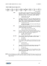
USART2 has a clock polarity bit (UCPOL) and a clock phase control bit (UCPHA) to select one of four
clock formats for data transfers. UCPOL selectively inserts an inverter in series with a clock. UCPHA
selects one of two different clock phase relationships between the clock and the data. Note that UCPHA
and UCPOL bits in UCTRL1 register have different meanings according to the UMSEL[1:0] bits which
decides the operating mode of USART2.
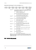
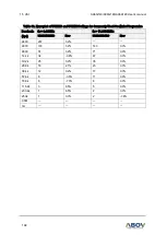
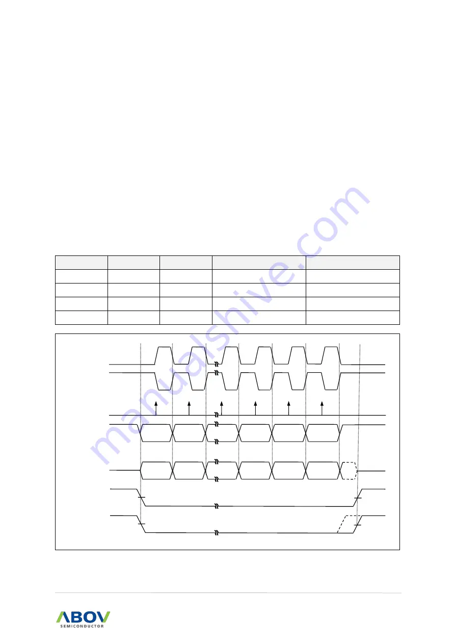
Table 34 shows four combinations of UCPOL and UCPHA for SPI mode 0, 1, 2, and 3.
Table 35. CPOL Functionality
SPI Mode
UCPOL
UCPHA
Leading Edge
Trailing Edge
0
0
0
Sample (Rising)
Setup (Falling)
1
0
1
Setup (Rising)
Sample (Falling)
2
1
0
Sample (Falling)
Setup (Rising)
3
1
1
Setup (Falling)
Sample (Rising)
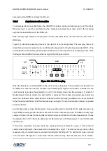
Figure 108. SPI Clock Formats when UCPHA = 0
XCK
(UCPOL=1)
MISO
MOSI
XCK
(UCPOL=0)
/SS OUT
(MASTER)
BIT7
BIT0
/SS IN
(SLAVE)
BIT6
BIT1
…
…
BIT2
BIT5
BIT0
BIT7
BIT1
BIT6
SAMPLE
MSB First
LSB First


