background image

A96G140/A96G148/A96A148 User’s manual


4. Central processing unit ABOV 


29 

4


Central Processing Unit (CPU) 

Central  Processing  Unit  (CPU)  of  A96G140/A96G148/A96A148  is  based  on  Mentor  Graphics 
M8051EW core, which offers improved code efficiency and high performance. 

4.1


Architecture and registers 

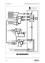
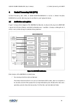
Figure 10 shows a block diagram of the M8051EW architecture. As shown in the figure, the M8051EW 
supports both Program Memory and External Data Memory. In addition, it features a Debug Mode in 
which it can be driven through a dedicated debug interface. 


Figure 10. M8051EW Architecture 

Main features of the M8051EW are listed below: 


Two clocks per machine cycle architecture: 

This allows the device either to run up to six times faster with the same power consumption or 
to consume one sixth of the power when running at standard speed. All instructions have zero-
wait-state execution times that are exactly 1/6 of the time each standard part takes. 


Summary of Contents for A96A148

Page 1: ...ncorporates followings to offer highly flexible and cost effective solutions 64Kbytes of FLASH 256bytes of IRAM 2304bytes of XRAM general purpose I O basic interval timer watchdog timer 8 16 bit timer...

Page 2: ...47 6 1 Port register 47 6 1 1 Data register Px 47 6 1 2 Direction register PxIO 47 6 1 3 Pull up register selection register PxPU 47 6 1 4 Open drain Selection Register PxOD 47 6 1 5 De bounce Enable...

Page 3: ...6 Interrupt register description 75 8 Clock generator 82 8 1 Clock generator block diagram 82 8 2 Register map 83 8 3 Register description 83 9 Basic interval timer 86 9 1 BIT block diagram 86 9 2 BIT...

Page 4: ...38 12 6 Timer 5 141 12 6 1 16 bit timer counter mode 141 12 6 2 16 bit capture mode 143 12 6 3 16 bit PPG mode 144 12 6 4 16 bit timer 5 block diagram 147 12 6 5 Register map 147 12 6 6 Register descr...

Page 5: ...eiver 177 15 19 3USIn I2C slave transmitter 178 15 19 4USIn I2C slave receiver 179 15 20 USIn I2C block diagram 181 15 21 Register map 181 15 22 USIn register description 182 15 23 Baud rate settings...

Page 6: ...rial in system program mode 240 19 3 1 Flash operation 240 19 4 Mode entrance method of ISP mode 246 19 4 1 Mode entrance method for ISP 246 19 5 Security 247 19 6 Configure option 247 20 Development...

Page 7: ...e Timing Diagram 73 Figure 23 Correspondence between Vector Table Address and the Entry Address of ISR 73 Figure 24 Saving Restore Process Diagram and Sample Source 73 Figure 25 Timing Chart of Interr...

Page 8: ...imer Counter Mode of Timer 5 142 Figure 71 16 bit Timer Counter Mode Operation Example 142 Figure 72 16 bit Capture Mode of Timer 5 143 Figure 73 16 bit Capture Mode Operation Example 144 Figure 74 Ex...

Page 9: ...ESET 226 Figure 121 Oscillator generating waveform example 226 Figure 122 Block Diagram of LVR 227 Figure 123 Internal Reset at Power Fail Situation 227 Figure 124 Configuration Timing When LVR RESET...

Page 10: ...List of figures A96G140 A96G148 A96A148 User s manual 10...

Page 11: ...egister Map 138 Table 25 TIMER 5 Operating Modes 141 Table 26 TIMER 5 Register Map 147 Table 27 Buzzer Frequency at 8MHz 150 Table 28 Buzzer Driver Register Map 151 Table 29 ADC Register Map 155 Table...

Page 12: ...erfaces by Series 251 Table 52 Feature Comparison Chart By Series and Core 252 Table 53 OCD Type of Each Series 253 Table 54 Comparison of OCD 1 and OCD 2 253 Table 55 Interrupt Priorities in Groups a...

Page 13: ...ription Core CPU 8 bit CISC core M8051 2 clocks per cycle Interrupt Up to 23 peripheral interrupts supported EINT0 to 7 EINT8 EINT10 EINT11 EINT12 5 Timer 0 1 2 3 4 5 6 WDT 1 BIT 1 WT 1 USART Rx Tx 2...

Page 14: ...5 ch T1 T2 T3 T4 T5 Communication function USART2 8 bit USART x 1 ch or 8 bit SPI x 1 ch Receiver timer out RTO 0 error baud rate USI0 1 USART SPI I2C 8 bit USART x 2 ch or 8 bit SPI x 2 ch or I2C x...

Page 15: ...manual 1 Description 15 Table 1 A96G140 A96G148 A96A148 Device Features and Peripheral Counts continued Peripherals Description Package Pb free packages 48 LQFP 7x7 mm 48 QFN 6x6 mm 44 MQFP 10x10 mm...

Page 16: ...ator Power down mode Clock generator 32MHz Internal RC OSC 128kHz Internal RC OSC 12MHz Crystal OSC 32 768kHz Crystal OSC Buzzer 1 channel 8 bit UART 3 channels 8 bit SPI 3 channels 8 bit I2C 2 channe...

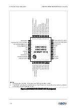
Page 17: ...escription In this chapter A96G140 A96G148 A96A148 device pinouts and pin descriptions are introduced 2 1 Pinouts A96G140CL A96G148CL 48LQFP 0707 A96G140CU A96G148CU 48QFN 0606 NOTE Programmer E PGM E...

Page 18: ...G148SQ 44MQFP 1010 NOTES 1 The programmer E PGM E Gang4 6 uses P0 1 0 pin as DSCL DSDA 2 The P44 P47 pins should be selected as a push pull output or an input with pull up resistor by software control...

Page 19: ...LQFP NOTES 1 The programmer E PGM E Gang4 6 uses P0 1 0 pin as DSCL DSDA 2 The P14 P17 P23 P25 P34 P37 and P43 P47 pins should be selected as a push pull output or an input with pull up resistor by so...

Page 20: ...pull output or an input with pull up resistor by software control when the 32 pin package is used Figure 5 A96G140 A96G148 32SOP Pin Assignment 1 2 13 14 8 9 10 11 12 3 4 5 6 7 16 15 21 20 19 18 17 26...

Page 21: ...03 AN1 EINT1 P02 AN0 AVREF EINT0 T4O PWM4O P30 LED7 P20 AN14 TXD1 SDA1 MOSI1 VDD P05 AN3 EINT3 EC3 P04 AN2 EINT2 T3O PWM3O P07 AN5 EINT5 P11 AN12 EINT12 T2O PWM2O P12 AN11 EINT11 T1O PWM1O P10 AN13 RX...

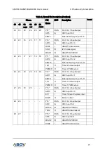
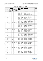
Page 22: ...rt 0 bit 2 Input output AN0 IA ADC input ch 0 AVREF P A D converter reference voltage EINT0 I External interrupt input ch 0 T4O O Timer 4 interval output PWM4O O Timer 4 PWM output 37 34 24 28 24 24 P...

Page 23: ...S Port 1 bit 1 Input output AN12 IA ADC input ch 12 EINT12 I External interrupt input ch 12 T2O O Timer 2 interval output PWM2O O Timer 2 PWM output 26 24 18 22 19 19 P12 IOUS Port 1 bit 2 Input outpu...

Page 24: ...I 21 20 14 18 15 P21 IOUS Port 2 bit 1 Input output AN15 IA ADC input ch 15 SCK1 IO USART1 clock signal 20 19 13 17 P22 IOUS Port 2 bit 2 Input output SS1 IO USART1 slave select signal 19 18 P23 IOU P...

Page 25: ...ART0 SPI MISO 3 3 5 9 9 P41 IOUS Port 4 bit 1 Input output TXD0 O USART0 data transmit SDA0 IO I2C data signal MOSI0 IO USART0 SPI MOSI 4 4 10 10 P42 IOUS Port 4 bit 2 Input output SCK0 IO USART0 cloc...

Page 26: ...not in the 32 pin package 2 The P13 P17 P22 P27 P34 P37 and P43 P47 are not in the 28 pin package 3 The P43 is not in the 48 pin package 4 The P55 RESETB pin is configured as one of the P55 and RESET...

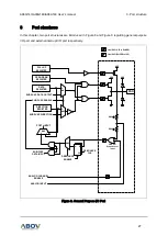
Page 27: ...respectively PULL UP REGISTER OPEN DRAIN REGISTER DATA REGISTER SUB FUNC DATA OUTPUT SUB FUNC ENABLE DIRECTION REGISTER SUB FUNC DIRECTION Q D r CP DEBOUNCE CLK DEBOUNCE ENABLE SUB FUNC DATA INPUT POR...

Page 28: ...to 1 8V DATA REGISTER OPEN DRAIN REGISTER PULL UP REGISTER SUB FUNC DATA OUTPUT DIRECTION REGISTER SUB FUNC DIRECTION 0 1 MUX MUX 0 1 0 1 MUX r D CP Q DEBOUNCE CLK DEBOUNCE ENABLE PORTx INPUT SUB FUN...

Page 29: ...figure the M8051EW supports both Program Memory and External Data Memory In addition it features a Debug Mode in which it can be driven through a dedicated debug interface Figure 10 M8051EW Architect...

Page 30: ...interfaces Up to 256bytes of Internal Data Memory Up to 1Mbyte of RAM or ROM Program Memory accessible by selecting one from interfaces Support for synchronous and asynchronous Program External Data...

Page 31: ...isters Four banks of registers are available The current bank is selected by the 3rd and 4th bits of the PSW 4 Register specific addressing mode In this mode some instructions only operate on specific...

Page 32: ...Memory where this is implemented as RAM This instruction can also be used subsequently to modify contents of the Program Memory RAM Arithmetic Instruction The M8051EW implements ADD ADDC Add with Car...

Page 33: ...s instruction jumps to a location of which address is stored in DPTR register and offset by a value stored in the accumulator Subroutine calls and returns There are only two sorts of subroutine call A...

Page 34: ...148 has just 64Kbytes program memory space Figure 9 shows a map of the lower part of the program memory After reset CPU begins execution from location 0000H Each interrupt is assigned a fixed location...

Page 35: ...mory space Thus as shown in figure 10 the upper 128bytes and SFR space occupy the same block of addresses 80H through FFH although they are physically separate entities The lower 128bytes of RAM are p...

Page 36: ...irect addressing The upper 128bytes of RAM can only be accessed by indirect addressing These spaces are used for data RAM and stack FFH 80H 7FH 00H FFH 80H Upper 128bytes Internal RAM Indirect Address...

Page 37: ...3 42 41 40 3F 3E 3D 3C 3B 3A 39 38 37 36 35 34 33 32 31 30 2F 2E 2D 2C 2B 2A 29 28 27 26 25 24 23 22 21 20 1F 1E 1D 1C 1B 1A 19 18 17 16 15 14 13 12 11 10 0F 0E 0D 0C 0B 0A 09 08 07 06 05 04 03 02 01...

Page 38: ...compatible 00H 8H 1 01H 9H 02H 0AH 03H 0BH 04H 0CH 05H 0DH 06H 0EH 07H 0FH 0F8H IP1 UBAUD UDATA P5FSR 0F0H B USI1ST1 USI1ST2 USI1BD USI1SDHR USI1DR USI1SCLR USI1SCHR 0E8H RSTFR USI1CR1 USI1CR2 USI1CR3...

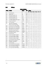
Page 39: ...DCDRH 90H P2 P0OD P1OD P2OD P4OD P5PU WTCR BUZCR 88H P1 WTDR WTCNT SCCR BITCR BITCNT WDTCR WDTDR WDTCNT BUZDR 80H P0 SP DPL DPH DPL1 DPH1 LVICR PCON NOTE 00H 8H these registers are bit addressable Tab...

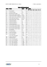
Page 40: ...ic Interval Timer Counter Register BITCNT R 0 0 0 0 0 0 0 0 8DH Watch Dog Timer Control Register WDTCR R W 0 0 0 0 0 8EH Watch Dog Timer Data Register WDTDR W 1 1 1 1 1 1 1 1 Watch Dog Timer Counter R...

Page 41: ...0 0 0 0 ACH P0 Pull up Resistor Selection Register P0PU R W 0 0 0 0 0 0 0 0 ADH P1 Pull up Resistor Selection Register P1PU R W 0 0 0 0 0 0 0 0 AEH P2 Pull up Resistor Selection Register P2PU R W 0 0...

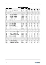
Page 42: ...W 0 0 0 0 0 0 0 0 CDH USART Control Register 3 UCTRL3 R W 0 0 0 0 0 0 0 CFH USART Status Register USTAT R W 1 0 0 0 0 0 0 0 D0H Program Status Word Register PSW R W 0 0 0 0 0 0 0 0 D1H P5 Direction R...

Page 43: ...USI1 Control Register 3 USI1CR3 R W 0 0 0 0 0 0 0 0 ECH USI1 Control Register 4 USI1CR4 R W 0 0 0 0 0 EDH USI1 Slave Address Register USI1SAR R W 0 0 0 0 0 0 0 0 EEH Port3 Function Selection Register...

Page 44: ...1011H Timer 5 Control Low Register T5CRL R W 0 0 0 0 0 0 1012H Timer 5 A Data High Register T5ADRH R W 1 1 1 1 1 1 1 1 1013H Timer 5 A Data Low Register T5ADRL R W 1 1 1 1 1 1 1 1 1014H Timer 5 B Dat...

Page 45: ...egister SP Stack Pointer 81H 7 6 5 4 3 2 1 0 SP R W R W R W R W R W R W R W R W Initial value 07H SP Stack Pointer DPL Data Pointer Register Low 82H 7 6 5 4 3 2 1 0 DPL R W R W R W R W R W R W R W R W...

Page 46: ...rpose User Definable Flag RS1 Register Bank Select bit 1 RS0 Register Bank Select bit 0 OV Overflow Flag F1 User Definable Flag P Parity Flag Set Cleared by hardware each instruction cycle to indicate...

Page 47: ...set by a system reset 6 1 3 Pull up register selection register PxPU The on chip pull up resistor can be connected to I O ports individually with a pull up resistor selection register PxPU The pull up...

Page 48: ...D5H R W 00H P1 Function Selection High Register P1FSRL D4H R W 00H P1 Function Selection Low Register P2 90H R W 00H P2 Data Register P2IO B9H R W 00H P2 Direction Register P2PU AEH R W 00H P2 Pull up...

Page 49: ...ster 80H 7 6 5 4 3 2 1 0 P07 P06 P05 P04 P03 P02 P01 P00 R W R W R W R W R W R W R W R W Initial value 00H P0 7 0 I O Data P0IO P0 Direction Register A1H 7 6 5 4 3 2 1 0 P07IO P06IO P05IO P04IO P03IO...

Page 50: ...1 fx 4 1 0 fx 4096 1 1 LSIRC 128KHz P07DB Configure De bounce of P07 Port 0 Disable 1 Enable P06DB Configure De bounce of P06 Port 0 Disable 1 Enable P05DB Configure De bounce of P05 Port 0 Disable 1...

Page 51: ...when input 0 1 reserved 1 0 AN5 Function 1 1 Reserved P0FSRH 5 4 P06 Function Select P0FSRH5 P0FSRH4 Description 0 0 I O Port EINT4 function possible when input 0 1 reserved 1 0 AN4 Function 1 1 PWM5...

Page 52: ...REF Function 1 0 AN0 Function 1 1 T4O PWM4O Function P0FSRL 3 2 P01 Function Select P0FSRL3 P0FSRL2 Description 0 0 I O Port 0 1 T3O PWM3O Function 1 0 reserved 1 1 TXD2 Function P0FSRL 1 0 P00 Functi...

Page 53: ...Direction 0 Input 1 Output NOTE EINT6 EINT7 EINT11 EINT12 EC1 function possible when input P1PU P1 Pull up Resistor Selection Register ADH 7 6 5 4 3 2 1 0 P17PU P16PU P15PU P14PU P13PU P12PU P11PU P1...

Page 54: ...P16 Port 0 Disable 1 Enable P12DB Configure De bounce of P12 Port 0 Disable 1 Enable P11DB Configure De bounce of P11 Port 0 Disable 1 Enable NOTES 1 If the same level is not detected on enabled pin...

Page 55: ...tion 0 0 I O Port EINT6 function possible when input 0 1 reserved 1 0 AN6 Function 1 1 SS2 Function P1FSRH 5 4 P16 Function Select P1FSRH5 P1FSRH4 Description 0 0 I O Port EINT7 function possible when...

Page 56: ...nput 0 1 reserved 1 0 AN11 Function 1 1 T1O PWM1O Function P1FSRL 3 2 P11 Function Select P1FSRL3 P1FSRL2 Description 0 0 I O Port EINT12 function possible when input 0 1 reserved 1 0 AN12 Function 1...

Page 57: ...l value 00H P2IO 7 0 P2 Data I O Direction 0 Input 1 Output P2PU P2 Pull up Resistor Selection Register AEH 7 6 5 4 3 2 1 0 P27PU P26PU P25PU P24PU P23PU P22PU P21PU P20PU R W R W R W R W R W R W R W...

Page 58: ...R 1 0 P20 Function Select P2FSR1 P2FSR0 Description 0 0 I O Port 0 1 reserved 1 0 AN14 Function 1 1 TXD1 SDA1 MOSI1 Function 6 5 P3 port 6 5 1 P3 port description P3 is an 8 bit I O port P3 control re...

Page 59: ...31IO P30IO R W R W R W R W R W R W R W R W Initial value 00H P3IO 7 0 P3 Data I O Direction 0 Input 1 Output P3PU P3 Pull up Resistor Selection Register AFH 7 6 5 4 3 2 1 0 P37PU P36PU P35PU P34PU P33...

Page 60: ...33 Function select 0 I O Port 1 LED4 Function P3FSR2 P32 Function Select 0 I O Port 1 LED5 Function P3FSR1 P31 Function select 0 I O Port 1 LED6 Function P3FSR0 P30 Function Select 0 I O Port 1 LED7 F...

Page 61: ...l value 00H P4IO 7 0 P4 Data I O Direction 0 Input 1 Output P4PU P4 Pull up Resistor Selection Register A3H 7 6 5 4 3 2 1 0 P47PU P46PU P45PU P44PU P43PU P42PU P41PU P40PU R W R W R W R W R W R W R W...

Page 62: ...1 P5 port description P5 is a 6 bit I O port P5 control registers consist of P5 data register P5 P5 direction register P5IO andP5 pull up resistor selection register P5PU Refer to the port function s...

Page 63: ...al value 00H P5FSR 7 6 P54 Function Select P5FSR7 P5FSR6 Description 0 0 I O Port EINT10 function possible when input 0 1 SXOUT Function 1 0 reserved 1 1 reserved P5FSR 5 4 P53 Function Select P5FSR5...

Page 64: ...four pairs of interrupt enable registers IE IE1 IE2 and IE3 Each bit of IE IE1 IE2 IE3 register individually enables disables the corresponding interrupt source Overall control is provided by bit 7 o...

Page 65: ...Interrupt 5 Interrupt 11 Interrupt 17 Interrupt 23 Highest Lowest Highest Lowest Figure 15 Interrupt Group Priority Level 7 1 External interrupt External interrupts on INT0 INT1 INT5 INT6 and INT11 p...

Page 66: ...FLAG1 EINT2 Pin FLAG2 FLAG3 EINT4 Pin FLAG4 FLAG5 EINT6 Pin FLAG6 FLAG7 EINT11 Pin FLAG11 EINT12 Pin FLAG12 EIPOL1 2 2 EIPOL0H EIPOL0L 2 2 2 2 2 2 INT1 Interrupt INT11 Interrupt INT5 Interrupt EINT10...

Page 67: ...Timer 0 overflow Timer 0 Timer 1 Timer 2 Timer 3 IP1 IP IE FLAG10 FLAG11 IE2 T0OVIFR T0IFR T1IFR T2IFR T3IFR FLAG0 FLAG1 FLAG2 FLAG3 FLAG4 FLAG5 FLAG6 FLAG7 EIPOL1 USI0 I2C USI0 Rx USI0 Tx IE1 I2C0IFR...

Page 68: ...le 0033H USART2 TX Interrupt INT7 IE1 1 8 Maskable 003BH USI0 I2C Interrupt INT8 IE1 2 9 Maskable 0043H USI0 Rx Interrupt INT9 IE1 3 10 Maskable 004BH USI0 Tx Interrupt INT10 IE1 4 11 Maskable 0053H E...

Page 69: ...ceptance always generates at last cycle of the instruction So instead of fetching the current instruction CPU executes internally LCALL instruction and saves the PC at stack For the interrupt service...

Page 70: ...IE3 Saves PC value in order to continue process again after executing ISR IE EA Flag 0 1 Program Counter low Byte SP SP 1 M SP PCL 2 Program Counter high Byte SP SP 1 M SP PCH 3 Interrupt Vector Addre...

Page 71: ...multaneously the request of higher priority level is served first If more than one interrupt request are received the interrupt polling sequence determines which request is served first by hardware Ho...

Page 72: ...rved after the INT1 service has completed An interrupt service routine may be only interrupted by an interrupt of higher priority and if two interrupts of different priority occur at the same time the...

Page 73: ...the Entry Address of ISR 7 9 Saving restore general purpose registers Figure 24 Saving Restore Process Diagram and Sample Source Interrupt latched Interrupt goes active System Clock Max 4 Machine Cycl...

Page 74: ...es long call to jump to interrupt service routine 7 11 Interrupt register overview 7 11 1 Interrupt Enable Register IE IE1 IE2 and IE3 Interrupt enable register consists of global interrupt control bi...

Page 75: ...POL0H L and External Interrupt Polarity1 Register EIPOL1 determines an edge type from rising edge falling edge and both edges of interrupt Initially default value is no interrupt at any edge 7 11 5 Re...

Page 76: ...nterrupt disable 1 All Interrupt enable INT5E Enable or Disable External Interrupt 0 7 EINT0 EINT7 0 Disable 1 Enable INT4E Enable or Disable USI1 Tx Interrupt 0 Disable 1 Enable INT3E Enable or Disab...

Page 77: ...0H INT11E Enable or Disable External Interrupt 12 EINT12 0 Disable 1 Enable INT10E Enable or Disable USI0Tx Interrupt 0 Disable 1 Enable INT9E Enable or Disable USI0 Rx Interrupt 0 Disable 1 Enable IN...

Page 78: ...Enable or Disable Timer 4 5 Match Interrupt 0 Disable 1 Enable INT16E Enable or Disable Timer 3 Match Interrupt 0 Disable 1 Enable INT15E Enable or Disable Timer 2 Match Interrupt 0 Disable 1 Enable I...

Page 79: ...e 1 Enable INT20E Enable or Disable WT Interrupt 0 Disable 1 Enable INT19E Enable or Disable USART2 RX Interrupt 0 Disable 1 Enable INT18E Enable or Disable ADC Interrupt 0 Disable 1 Enable IP Interru...

Page 80: ...3 2 1 0 POL7 POL6 POL5 POL4 R W R W R W R W R W R W R W R W Initial value 00H EIPOL0H 7 0 External interrupt EINT7 EINT6 EINT5 EINT4 polarity selection POLn 1 0 Description 0 0 No interrupt at any edg...

Page 81: ...y INT_ACK signal Writing 1 has no effect 0 T0 Interrupt no generation 1 T0 Interrupt generation EIFLAG1 3 0 When an External Interrupt EINT8 EINT10 EINT12 is occurred the flag becomes 1 The flag is cl...

Page 82: ...e external clock signal into the XIN SXIN pin and open XOUT SXOUT pin Default system clock is 1MHz INT RC Oscillator To stabilize the system internally 128KHz LOW INT RC oscillator on POR is recommend...

Page 83: ...26 Clock Generator Block Diagram 8 2 Register map Table 10 Clock Generator Register Map Name Address Direction Default Description SCCR 8AH R W 00H System and Clock Control Register OSCCR C8H R W 28H...

Page 84: ...st divider Selection IRCS2 IRCS1 IRCS0 Description 0 0 0 INT RC 64 0 5MHz 0 0 1 INT RC 32 1MHz 0 1 0 INT RC 16 2MHz 0 1 1 INT RC 8 4MHz 1 0 0 INT RC 4 8MHz 1 0 1 INT RC 2 16MHz 1 1 0 Test only Other V...

Page 85: ...s 4MHz MX_FIL_DIS Main X TAL noise canceller selection 0 Using noise filter 1 Bypass noise filter MX_ISEL 1 0 Current selective option for MX TAL MX_ISEL1 MX_ISEL0 Description 0 0 HIGH 12M 0 1 MID HIG...

Page 86: ...9 1 BIT block diagram In this section basic interval timer of A96G140 A96G148 A96A148 is described in a block diagram 32 Prescaler 1 4096 1 16 1 1024 1 128 3 BITCK BITCNT BITIFR Overflow 8 bit up coun...

Page 87: ...bit becomes 1 For clearing bit write 0 to this bit or auto clear by INT_ACK signal Writing 1 has no effect 0 BIT interrupt no generation 1 BIT interrupt generation BITCK 2 0 Select BIT clock source BI...

Page 88: ...ng WDTCR 6 bit If WDTCR 5 is set to 1 the WDT counter value is cleared and counts up After 1 machine cycle this bit is cleared to 0 automatically The WDT consists of an 8 bit binary counter and a watc...

Page 89: ...WDTCK Figure 29 Watch Dog Timer Block Diagram 10 3 Register map Table 12 Watchdog Timer Register Map Name Address Direction Default Description WDTCNT 8EH R 00H Watch Dog Timer Counter Register WDTDR...

Page 90: ...2 1 0 WDTEN WDTRSON WDTCL WDTCK WDTIFR R W R W R W R W R W Initial value 00H WDTEN Control WDT Operation 0 Disable 1 Enable WDTRSON Control WDT RESET Operation 0 Free Running 8 bit timer 1 Watch Dog...

Page 91: ...nter circuits may be composed of 21 bit counter which contains low 14 bit with binary counter and high 7 bit counter in order to increase resolution In WTDR it can control WT clear and set interval va...

Page 92: ...TCNT Watch Timer Counter Register Read Case 89H 7 6 5 4 3 2 1 0 WTCNT6 WTCNT5 WTCNT4 WTCNT3 WTCNT2 WTCNT1 WTCNT0 R R R R R R R Initial value 00H WTCNT 6 0 WT Counter WTDR Watch Timer Data Register Wri...

Page 93: ...e 0 to this bit or automatically clear by INT_ACK signal Writing 1 has no effect 0 WT Interrupt no generation 1 WT Interrupt generation WTIN 1 0 Determine interrupt interval WTIN1 WTIN0 Description 0...

Page 94: ...T0DR T0O port toggles In addition timer 0 outputs PWM waveform through PWM0O port in the PWM mode Table 14 Timer 0 Operating Mode T0EN T0MS 1 0 T0CK 2 0 Timer 0 1 00 XXX 8 bit Timer Counter Mode 1 01...

Page 95: ...0 T0EN 8 bit Timer 0 Counter T0DR 8Bit Comparator T0IFR T0O PWM0O 8 bit Timer 0 Data Register INT_ACK Clear Match signal Clear Match MUX T0MS 1 0 2 To interrupt block T0EN T0MS1 T0MS0 T0CK2 T0CK1 T0C...

Page 96: ...pt of timer 0 occurs In PWM mode the match signal does not clear the counter Instead it runs continuously overflowing at FFH Then the counter continues incrementing from 00H The timer 0 overflow inter...

Page 97: ...T0CNT T0PWM 00H 01H 02H 4AH FFH FEH 00H T0 Match Interrupt T0 Overflow Interrupt T0DR 1 T0DR 4AH Timer 0 clock Set T0EN T0PWM T0 Match Interrupt 2 T0DR 00H T0PWM T0 Match Interrupt 3 T0DR FFH PWM Mode...

Page 98: ...timer 0 output T0O waveform is not available According to EIPOL1 registers setting the external interrupt EINT10 function is chosen Of course the EINT10 pin must be set to an input port T0CDR and T0D...

Page 99: ...A96G140 A96G148 A96A148 User s manual 12 Timer 0 1 2 3 4 5 99 Figure 36 Input Capture Mode Operation for Timer 0 Figure 37 Express Timer Overflow in Capture Mode...

Page 100: ...EIPOL1 1 0 FLAG10 EIFLAG1 0 INT_ACK Clear To interrupt block 2 T0MS 1 0 2 T0MS 1 0 2 Match signal T0CC Figure 38 8 bit Timer 0 Block Diagram 12 1 5 Register map Table 15 Timer 0 Register Map Name Add...

Page 101: ...0CK0 T0CC R W R W R W R W R W R W R W Initial value 00H T0EN Control Timer 0 0 Timer 0 disable 1 Timer 0 enable T0MS 1 0 Control Timer 0 Operation Mode T0MS1 T0MS0 Description 0 0 Timer counter mode 0...

Page 102: ...mode In addition Timer 1 outputs PWM waveform through PWM1Oport in the PPG mode Table 16 TIMER 1 Operating Modes T1EN P1FSRL 5 4 T1MS 1 0 T1CK 2 0 Timer 1 1 11 00 XXX 16 Bit Timer Counter Mode 1 00 01...

Page 103: ...1CNTL Clear Edge Detector T1ECE EC1 Comparator 16 bit A Data Register T1ADRH T1ADRL T1IFR INT_ACK Clear To interrupt block A Match Buffer Register A A Match T1CC Reload Pulse Generator T1O R T1EN 3 T1...

Page 104: ...H T1BDRL According to EIPOL1 registers setting the external interrupt EINT11 function is selected EINT11 pin must be set as an input port A Match T1CC T1EN P r e s c a l e r fx M U X fx 2 fx 4 fx 64 f...

Page 105: ...TIMER 1 has a PPG Programmable Pulse Generation function In PPG mode T1O PWM1O pin outputs up to 16 bit resolution PWM output For this function T1O PWM1O pin must be configured as a PWM output by sett...

Page 106: ...parator 16 bit A Data Register T1ADRH T1ADRL T1IFR INT_ACK Clear To interrupt block A Match Buffer Register A Reload Pulse Generator T1O PWM1O R T1EN 3 T1CK 2 0 2 T1EN T1CRH 1 ADDRESS BBH INITIAL VALU...

Page 107: ...3 7 2 M A Match 1 T1BDRH L 5 T1ADRH L PWM1O A Match 2 T1BDRH L T1ADRH L PWM1O A Match 3 T1BDRH L 0000H Low Level X 1 2 4 5 6 8 M 1 0 Timer 1 clock Counter T1ADRH L T1 Interrupt PWM1O B Match One shot...

Page 108: ...r Register A Reload Pulse Generator T1O PWM1O R EINT11 T1CNTR T1EN 3 T1CK 2 0 Clear EIPOL1 5 4 FLAG11 EIFLAG1 2 INT_ACK Clear To interrupt block 2 2 T1MS 1 0 2 Edge Detector T1ECE EC1 To Timer 2 block...

Page 109: ...2 T1ADRL1 T1ADRL0 R W R W R W R W R W R W R W R W Initial value FFH T1ADRL 7 0 T1 A Data Low Byte NOTE Do not write 0000H in the T1ADRH T1ADRL register when PPG mode T1BDRH Timer 1 B Data High Registe...

Page 110: ...imer 1 disable 1 Timer 1 enable Counter clear and start T1MS 1 0 Control Timer 1 Operation Mode T1MS1 T1MS0 Description 0 0 Timer counter mode T1O toggle at A match 0 1 Capture mode The A match interr...

Page 111: ...tion 1 T1 Interrupt generation T1POL T1O PWM1O Polarity Selection 0 Start High T1O PWM1O is low level at disable 1 Start Low T1O PWM1O is high level at disable T1ECE Timer 1 External Clock Edge Select...

Page 112: ...perating Modes T2EN P1FSRL 3 2 T2MS 1 0 T2CK 2 0 Timer 2 1 11 00 XXX 16 Bit Timer Counter Mode 1 00 01 XXX 16 Bit Capture Mode 1 11 10 XXX 16 Bit PPG Mode one shot mode 1 11 11 XXX 16 Bit PPG Mode rep...

Page 113: ...INT_ACK Clear To interrupt block A Match Buffer Register A Reload Pulse Generator T2O R T2EN 3 T2CK 2 0 2 A Match T2CC T2EN T2EN T2CRH 1 ADDRESS C3H INITIAL VALUE 0000_0000B T2MS1 T2MS0 T2CC 0 0 X T2C...

Page 114: ...er 2 output T2O waveform is not available According to EIPOL1 registers setting the external interrupt EINT12 function is selected EINT12 pin must be set as an input port A Match T2CC T2EN P r e s c a...

Page 115: ...A96G140 A96G148 A96A148 User s manual 12 Timer 0 1 2 3 4 5 115 Figure 49 16 bit Capture Mode Operation Example Figure 50 Express Timer Overflow in Capture Mode...

Page 116: ...x 512 fx 8 fx 1 Comparator 16 bit Counter T2CNTH T2CNTL 16 bit B Data Register T2BDRH T2BDRL Clear B Match T1 A Match Buffer Register B Comparator 16 bit A Data Register T2ADRH T2ADRL T2IFR INT_ACK Cl...

Page 117: ...3 7 2 M A Match 1 T2BDRH L 5 T2ADRH L PWM2O A Match 2 T2BDRH L T2ADRH L PWM2O A Match 3 T2BDRH L 0000H Low Level X 1 2 4 5 6 8 M 1 0 Timer 2 clock Counter T2ADRH L T2 Interrupt PWM2O B Match One shot...

Page 118: ...se Generator T2O PWM2O R EINT12 T2CNTR T2EN 3 T2CK 2 0 Clear EIPOL1 7 6 FLAG12 EIFLAG1 3 INT_ACK Clear To interrupt block 2 2 T2MS 1 0 2 T1 A Match A Match T2CC T2EN A Match T2CC T2EN NOTE T1 A Match...

Page 119: ...RL2 T2ADRL1 T2ADRL0 R W R W R W R W R W R W R W R W Initial value FFH T2ADRL 7 0 T2 A Data Low Byte NOTE Do not write 0000H in the T2ADRH T2ADRL register when PPG mode T2BDRH Timer 2 B Data High Regis...

Page 120: ...r 2ControlLow Register C2H 7 6 5 4 3 2 1 0 T2CK2 T2CK1 T2CK0 T2IFR T2POL T2CNTR R W R W R W R W R W R W Initial value 00H T2CK 2 0 Select Timer 2 clock source fx is main system clock frequency T2CK2 T...

Page 121: ...on timer 3 outputs PWM waveform through PWM3O port in the PPG mode Table 20 TIMER 3 Operating Modes T3EN P0FSRH 1 0 T3MS 1 0 T3CK 2 0 Timer 3 1 11 00 XXX 16 Bit Timer Counter Mode 1 00 01 XXX 16 Bit C...

Page 122: ...TL Clear Edge Detector T3ECE EC3 Comparator 16 bit A Data Register T3ADRH T3ADRL T3IFR INT_ACK Clear To interrupt block A Match Buffer Register A A Match T3CC Reload Pulse Generator T3O R T3EN 2 T3MS1...

Page 123: ...result is loaded into T3BDRH T3BDRL According to EIPOL0L registers setting the external interrupt EINT3 function is selected EINT3 pin must be set as an input port A Match T3CC T3EN P r e s c a l e r...

Page 124: ...12 Timer 0 1 2 3 4 5 A96G140 A96G148 A96A148 User s manual 124 Figure 57 16 bit Capture Mode Operation Example Figure 58 Express Timer Overflow in Capture Mode...

Page 125: ...fx M U X fx 2 fx 4 fx 64 fx 512 fx 2048 fx 8 fx 1 Comparator 16 bit Counter T3CNTH T3CNTL 16 bit B Data Register T3BDRH T3BDRL Clear B Match Edge Detector T3ECE EC3 Buffer Register B Comparator 16 bi...

Page 126: ...3 7 2 M A Match 1 T3BDRH L 5 T3ADRH L PWM3O A Match 2 T3BDRH L T3ADRH L PWM3O A Match 3 T3BDRH L 0000H Low Level X 1 2 4 5 6 8 M 1 0 Timer 3 clock Counter T3ADRH L T3 Interrupt PWM3O B Match One shot...

Page 127: ...A96G140 A96G148 A96A148 User s manual 12 Timer 0 1 2 3 4 5 127...

Page 128: ...ster A Reload Pulse Generator T3O R EINT3 T3CNTR T3EN Clear EIPOL0L 7 6 FLAG3 EIFLAG0 3 INT_ACK Clear To interrupt block 2 2 T3MS 1 0 2 Edge Detector T3ECE EC3 To Timer 4 block A Match T3CC T3EN A Mat...

Page 129: ...2 T3ADRL1 T3ADRL0 R W R W R W R W R W R W R W R W Initial value FFH T3ADRL 7 0 T3 A Data Low Byte NOTE Do not write 0000H in the T3ADRH T3ADRL register when PPG mode T3BDRH Timer 3 B Data High Registe...

Page 130: ...Timer 3 disable 1 Timer 3 enable Counter clear and start T3MS 1 0 Control Timer 3 Operation Mode T3MS1 T3MS0 Description 0 0 Timer counter mode T3O toggle at A match 0 1 Capture mode The A match inte...

Page 131: ...ration 1 T3 Interrupt generation T3POL T3O PWM3O Polarity Selection 0 Start High T3O PWM3O is low level at disable 1 Start Low T3O PWM3O is high level at disable T3ECE Timer 3 External Clock Edge Sele...

Page 132: ...ing Modes T4EN P0FSRH 3 2 T4MS 1 0 T4CK 2 0 Timer 4 1 11 00 XXX 16 Bit Timer Counter Mode 1 00 01 XXX 16 Bit Capture Mode 1 11 10 XXX 16 Bit PPG Mode one shot mode 1 11 11 XXX 16 Bit PPG Mode repeat m...

Page 133: ...Clear To interrupt block A Match Buffer Register A Reload Pulse Generator T4O R T4EN 3 T4CK 2 0 2 A Match T4CC T4EN T4EN T4CRH 1 ADDRESS 1008H INITIAL VALUE 0000_0000B T4MS1 T4MS0 T4CC 0 0 X T4CK2 T4...

Page 134: ...timer 4 output T4O waveform is not available According to EIPOL0L registers setting the external interrupt EINT4 function is selected EINT4 pin must be set as an input port A Match T4CC T4EN P r e s c...

Page 135: ...A96G140 A96G148 A96A148 User s manual 12 Timer 0 1 2 3 4 5 135 Figure 65 16 bit Capture Mode Operation Example Figure 66 Express Timer Overflow in Capture Mode...

Page 136: ...x 512 fx 8 fx 1 Comparator 16 bit Counter T4CNTH T4CNTL 16 bit B Data Register T4BDRH T4BDRL Clear B Match T3 A Match Buffer Register B Comparator 16 bit A Data Register T4ADRH T4ADRL T4IFR S W Clear...

Page 137: ...3 7 2 M A Match 1 T4BDRH L 5 T4ADRH L PWM4O A Match 2 T4BDRH L T4ADRH L PWM4O A Match 3 T4BDRH L 0000H Low Level X 1 2 4 5 6 8 M 1 0 Timer 4 clock Counter T4ADRH L T4 Interrupt PWM4O B Match One shot...

Page 138: ...rator T4O R EINT4 T4CNTR T4EN 3 T4CK 2 0 Clear EIPOL0H 1 0 FLAG4 EIFLAG0 4 INT_ACK Clear To interrupt block 2 2 T4MS 1 0 2 T3 A Match A Match T4CC T4EN A Match T4CC T4EN PWM4O NOTE T3 A Match is a pul...

Page 139: ...RL2 T4ADRL1 T4ADRL0 R W R W R W R W R W R W R W R W Initial value FFH T4ADRL 7 0 T4 A Data Low Byte NOTE Do not write 0000H in the T4ADRH T4ADRL register when PPG mode T4BDRH Timer 4 B Data High Regis...

Page 140: ...unter T4CRL Timer 4 Control Low Register 1009H 7 6 5 4 3 2 1 0 T4CK2 T4CK1 T4CK0 T4IFR T4POL T4CNTR R W R W R W R W R W R W Initial value 00H T4CK 2 0 Select Timer 4 clock source fx is main system clo...

Page 141: ...enever counter value is equal to T5ADRH L T5O port toggles In addition the TIMER 5 outputs PWM waveform to PWM5O port in the PPG mode Table 24 TIMER 5 Operating Modes T5EN P0FSRH 5 4 T5MS 1 0 T5CK 2 0...

Page 142: ...a Register T5ADRH T5ADRL T5IFR S W Clear To interrupt block A Match Buffer Register A Reload Pulse Generator T5O R T5EN 3 T5CK 2 0 2 A Match T5CC T5EN T5EN T5CRH 1 ADDRESS 1010H INITIAL VALUE 0000_000...

Page 143: ...BDRH T5BDRL In the timer 5 capture mode timer 5 output T5O waveform is not available According to EIPOL0H registers setting the external interrupt EINT5 function is selected EINT5 pin must be set as a...

Page 144: ...148 A96A148 User s manual 144 Figure 73 16 bit Capture Mode Operation Example Figure 74 Express Timer Overflow in Capture Mode 12 6 3 16 bit PPG mode TIMER 5 has a PPG Programmable Pulse Generation fu...

Page 145: ...1 Comparator 16 bit Counter T5CNTH T5CNTL 16 bit B Data Register T5BDRH T5BDRL Clear B Match HIRC Buffer Register B Comparator 16 bit A Data Register T5ADRH T5ADRL T5IFR S W Clear To interrupt block...

Page 146: ...3 7 2 M A Match 1 T5BDRH L 5 T5ADRH L PWM5O A Match 2 T5BDRH L T5ADRH L PWM5O A Match 3 T5BDRH L 0000H Low Level X 1 2 4 5 6 8 M 1 0 Timer 5 clock Counter T5ADRH L T5 Interrupt PWM5O B Match One shot...

Page 147: ...atch Buffer Register A Reload Pulse Generator T5O R EINT5 T5CNTR T5EN 3 T5CK 2 0 Clear EIPOL0H 3 2 FLAG5 EIFLAG0 5 INT_ACK Clear To interrupt block 2 2 T5MS 1 0 2 HIRC A Match T5CC T5EN A Match T5CC T...

Page 148: ...RL2 T5ADRL1 T5ADRL0 R W R W R W R W R W R W R W R W Initial value FFH T5ADRL 7 0 T5 A Data Low Byte NOTE Do not write 0000H in the T5ADRH T5ADRL register when PPG mode T5BDRH Timer 5 B Data High Regis...

Page 149: ...r T5CRL Timer 5 Control Low Register 1011H 7 6 5 4 3 2 1 0 T5CK2 T5CK1 T5CK0 T5IFR T5POL T5CNTR R W R W R W R W R W R W Initial value 00H T5CK 2 0 Select Timer 5 clock source fx is main system clock f...

Page 150: ...e clock divided by prescaler Table 26 Buzzer Frequency at 8MHz BUZDR 7 0 Buzzer Frequency KHz BUZCR 2 1 00 BUZCR 2 1 01 BUZCR 2 1 10 BUZCR 2 1 11 0000_0000 125KHz 62 5KHz 31 25KHz 15 625KHz 0000_0001...

Page 151: ...BUZDR5 BUZDR4 BUZDR3 BUZDR2 BUZDR1 BUZDR0 R W R W R W R W R W R W R W R W Initial value FFH BUZDR 7 0 This bits control the Buzzer frequency Its resolution is 00H FFH BUZCR Buzzer Control Register 97...

Page 152: ...conversion is completed the result is loaded into ADCDRH and ADCDRL A D conversion status bit AFLAG is set to 1 and A D interrupt is set During the A D conversion AFLAG bit is read as 0 14 1 Conversi...

Page 153: ...N0 Reference Voltage AVREF AVSS AN1 AN2 AN14 AN15 ADCIFR AFLAG INT_ACK Clear Clear To interrupt block MUX VDD Start M U X T3 A match signal EXTINT0 7 REFSEL TRIG 2 0 3 ADST T1 A match signal EXTINT8 F...

Page 154: ...4 ADCDRH3 ADCDRH2 ADCDRH1 ADCDRH0 ADCDRL7 ADCDRL6 ADCDRL5 ADCDRL4 ADCO11 ADCO10 ADCO9 ADCO8 ADCO7 ADCO6 ADCO5 ADCO4 ADCO3 ADCO2 ADCO1 ADCO0 Align bit set 1 ADCDRH3 ADCDRH2 ADCDRH1 ADCDRH0 ADCDRL7 ADCD...

Page 155: ...R xxH A D Converter Data Low Register ADCCRH 9DH R W 01H A D Converter Control High Register ADCCRL 9CH R W 00H A D Converter Control Low Register 14 5 Register description ADCDRH A D Converter Data H...

Page 156: ...mes 1 For clearing bit write 0 to this bit or auto clear by INT_ACK signal Writing 1 has no effect 0 ADC Interrupt no generation 1 ADC Interrupt generation IREF Select internal voltage reference 0 Ext...

Page 157: ...ffect 1 ADC Conversion Start and auto clear REFSEL A D Converter Reference Selection 0 Internal Reference VDD 1 External Reference AVREF AFLAG A D Converter Operation State This bit is cleared to 0 wh...

Page 158: ...e USART SPI mode I2C mode 15 1 USIn UART mode Universal synchronous and asynchronous serial receiver and transmitter USART are highly flexible serial communication devices Main features are listed bel...

Page 159: ...e same frame formats as the transmitter and can detect frame error data overrun and parity errors 15 2 USIn UART block diagram RXDn Rx Control Clock Recovery Receive Shift Register RXSR Data Recovery...

Page 160: ...R1 register selects one from asynchronous operation and synchronous operation Asynchronous double speed mode is controlled by the DBLSn bit in the USInCR2 register The MASTERn bit in USInCR3 register...

Page 161: ...ve or clock output master Data sampling and transmitter are issued on the different edge of SCKn clock respectively For example if data input on RXDn MISOn in SPI mode pin is sampled on the rising edg...

Page 162: ...e 85 shows a possible combination of the frame formats Bits inside brackets are optional Figure 87 Frame Formats USIn 1 data frame consists of the following bits Idle No communication on communication...

Page 163: ...mitted When the shift register is loaded with new data it will transfer one complete frame according to the settings of control registers If the 9 bit characters are used in asynchronous or synchronou...

Page 164: ...nchronous or SPI operation mode the SCKn pin is used as transfer clock input so it should be selected to do SCKn function by P4FSR 5 4 and P2FSR 3 2 In SPI operation mode the SSn input pin in slave mo...

Page 165: ...as 0 This flag can be used for detecting out of sync conditions between data frames The data overrun DORn flag indicates data loss due to a receive buffer full condition DORn occurs when the receive...

Page 166: ...start bit is detected and the internally generated clock is synchronized to the incoming data frame And the data recovery can begin The synchronization process is repeated for each start bit As descri...

Page 167: ...In 15 10 USIn SPI mode The USIn can be set to operate in industrial standard SPI compliant mode The SPI mode has the following features Full duplex three wire synchronous data transfer Master and slav...

Page 168: ...relationships between the clock and data Note that CPHAn and CPOLn bits in USInCR1 register have different meanings according to the USInMS 1 0 bits which decides the operating mode of USIn Table 29 s...

Page 169: ...CKn edge The first SCKn edge shifts the first bit of data from the shifter onto the MOSIn output of the master and the MISOn output of the slave The next SCKn edge causes both the master and slave to...

Page 170: ...Rate Generator USInBD TXEn SCLK fx System clock MISOn MOSIn M U X MASTERn D E P FXCHn SCKn SCK Control MASTERn RXEn To interrupt block M U X Edge Detector And Controller SSn SS Control CPHAn CPOLn OR...

Page 171: ...SCLn SDAn lines that it will use the bus A STOP P condition is generated by the master to release the bus lines so that other devices can use it A high to low transition on the SDAn line while SCLn is...

Page 172: ...edge related clock pulse is generated by the master The transmitter releases the SDAn line HIGH during the acknowledge clock pulse The receiver must pull down the SDAn line during the acknowledge cloc...

Page 173: ...state until the clock HIGH state is reached However the LOW to HIGH transition of this clock may not change the state of the SCLn line if another clock is still within its LOW period In this way a sy...

Page 174: ...er is set it is cleared by writing any value to USInST2 When I2C interrupt occurs the SCLn line is hold LOW until writing any value to USInST2 When the IICnIFR flag is set the USInST2 contains a value...

Page 175: ...bit address and 1 bit transfer direction is transmitted to target slave device the master can know whether the slave acknowledged or not in the 9th high period of SCLn If the master gains bus masters...

Page 176: ...ly I2C generates TENDn interrupt I2C can choose one of the following cases regardless of the reception of ACK signal from slave Case 1 Master receives ACK signal from slave so continues data transfer...

Page 177: ...hen 7 bit address and 1 bit transfer direction is transmitted to target slave device the master can know whether the slave acknowledged or not in the 9th high period of SCLn If the master gains bus ma...

Page 178: ...To do this set ACKnEN bit in USInCR4 to ACKnowledge the next data to be received Case 2 Master wants to terminate data transfer when it receives next data by not generating ACK signal This can be don...

Page 179: ...I2C generates SSELn interrupt and the SCLn line is held LOW Note that even if the address equals to USInSLA 6 0 bits when the ACKnEN bit is disabled I2C enters idle state When SSELn interrupt occurs...

Page 180: ...o SLAn bits and the ACKnEN bit is enabled I2C generates SSELn interrupt and the SCLn line is held LOW Note that even if the address equals to SLAn bits when the ACKnEN bit is disabled I2C enters idle...

Page 181: ...block is an I2C mode and the corresponding port is a sub function for SCLn SDAn pin The SCLn SDAn pins are automatically set to the N channel open drain outputs and the input latch is read in the cas...

Page 182: ...ontrol Register 2 USI1CR3 EBH R W 00H USI1 Control Register 3 USI1CR4 ECH R W 00H USI1 Control Register 4 USI1ST1 F1H R W 80H USI1 Status Register 1 USI1ST2 F2H R 00H USI1 Status Register 2 15 22 USIn...

Page 183: ...l value 01H USInSDHR 7 0 The register is used to control SDAn output timing from the falling edge of SCI in I2C mode NOTES 1 That SDAn is changed after tSCLK X USInSDHR 2 in master SDAn change in the...

Page 184: ...is SCLK the system clock and the period is calculated by the formula tSCLK X 4 X USInSCLR 2 where tSCLK is the period of SCLK USInSAR USIn Slave Address Register For I2C mode DDH EDH n 0 1 7 6 5 4 3...

Page 185: ...ngth of data bits in frame USInS2 USInS1 USInS0 Data Length 0 0 0 5 bit 0 0 1 6 bit 0 1 0 7 bit 0 1 1 8 bit 1 0 0 Reserved 1 0 1 Reserved 1 1 0 Reserved 1 1 1 9 bit ORDn This bit in the same bit posit...

Page 186: ...se polling 1 When RXCn is set request an interrupt WAKEIEn Interrupt enable bit for asynchronous wake in STOP mode When device is in stop mode if RXDn goes to low level an interrupt can be requested t...

Page 187: ...CK is free running while UART is enabled in synchronous master mode 1 ACK is active while any frame is on transferring USInSSEN This bit controls the SSn pin operation only SPI mode 0 Disable 1 Enable...

Page 188: ...bit for I2C mode 0 Interrupt from I2C is inhibited use polling 1 Enable interrupt for I2C ACKnEN Controls ACK signal Generation at ninth SCLn period 0 No ACK signal is generated SDAn 1 1 ACK signal is...

Page 189: ...enerate an RXCn interrupt 0 There is no data unread in the receive buffer 1 There are more than 1 data in the receive buffer WAKEn This flag is set when the RXDn pin is detected low while the CPU is i...

Page 190: ...OP condition is detected 0 No STOP condition is detected 1 STOP condition is detected SSELn NOTE This bit is set when I2C is addressed by other master 0 I2C is not selected as a slave 1 I2C is address...

Page 191: ...0 25 0 2 47 0 0 51 0 2 4800 12 0 2 23 0 0 25 0 2 9600 6 7 0 11 0 0 12 0 2 14 4k 3 8 5 7 0 0 8 3 5 19 2k 2 8 5 5 0 0 6 7 0 28 8k 1 8 5 3 0 0 3 8 5 38 4k 1 18 6 2 0 0 2 8 5 57 6k 1 25 0 1 8 5 76 8k 1 0...

Page 192: ...Frequencies Baud rate bps fx 8 00MHz fx 11 0592MHz USI0BD USI1BD Error USI0BD USI1BD Error 2400 207 0 2 4800 103 0 2 143 0 0 9600 51 0 2 71 0 0 14 4k 34 0 8 47 0 0 19 2k 25 0 2 35 0 0 28 8k 16 2 1 23...

Page 193: ...Register Empty and RX Complete Double Speed Asynchronous Communication Mode USART2 has three main parts such as a Clock Generator Transmitter and Receiver Clock Generation logic consists of a synchro...

Page 194: ...bit Generator UDATA Tx SS2 SS Control RXC TXC UPM1 UPM0 USIZE2 USIZE1 USIZE0 UCPOL UCTRL1 ADDRESS CBH INITIAL VALUE 0000_0000B UDRIE TXCIE RXCIE TXE RXE U2X UCTRL2 ADDRESS CCH INITIAL VALUE 0000_0000...

Page 195: ...is controlled by the U2X bit in the UCTRL2 register The MASTER bit in UCTRL2 register controls whether the clock source is internal Master mode output port or external Slave mode input port The XCK pi...

Page 196: ...K is frequency of main system clock SCLK 16 4 Synchronous mode operation When synchronous mode or SPI mode is used the XCK pin will be used as either clock input slave or clock output master The depen...

Page 197: ...before the stop bits A high to low transition on data pin is considered as start bit When a complete frame is transmitted it can be directly followed by a new frame or the communication line can be s...

Page 198: ...7 1 Sending Tx data A data transmission is initiated by loading a transmit buffer UDATA register I O location with data to be transmitted The data written in the transmit buffer is moved to a shift re...

Page 199: ...er is disabled the TXD2 pin is used as normal General Purpose I O GPIO or primary function pin 16 8 USART2 receiver USART2 Receiver is enabled by setting the RXE bit in the UCTRL1 register When the Re...

Page 200: ...ved data from UDATA register read the USTAT register first which contains error flags Frame Error FE flag indicates the state of the first stop bit The FE flag is set when the stop bit was correctly d...

Page 201: ...9 and 10 for Normal mode and the samples 4 5 and 6 for Double Speed mode to decide if a valid start bit is received If more than 2 samples have logical low level it is considered that a valid start b...

Page 202: ...detection Figure 107 Stop Bit Sampling and Next Start Bit Sampling 16 9 SPI mode The USART2 can be set to operate in industrial standard SPI compliant mode The SPI mode has the following features Full...

Page 203: ...ock UCPHA selects one of two different clock phase relationships between the clock and the data Note that UCPHA and UCPOL bits in UCTRL1 register have different meanings according to the UMSEL 1 0 bit...

Page 204: ...but the data is not defined until the first XCK edge The first XCK edge shifts the first bit of data from the shifter onto the MOSI2 output of the master and the MISO2 output of the slave The next XCK...

Page 205: ...sysclk 16MHz Baud rate 115 200 bps Asynchronous Normal Mode U2X 0 Baud rate sysclk 16 x UBAUD 1 Calculated UBAUD 1000000 Target Baud rate 1 7 68 Error rate 0 68 UBAUD 8 Real baud rate at sysclk 16Mhz...

Page 206: ...ster UCTRL3 CDH R W 00H USART2 Control 3 Register UCTRL4 1018H R W 00H USART2 Control 4 Register USTAT CFH R 80H USART2 Status Register UBAUD FCH R W FFH USART2 Baud Rate Generation Register UDATA FDH...

Page 207: ...1 1 0 Reserved 1 1 1 9 bit UDORD This bit is in the same bit position with USIZE1 In SPI mode when set to one the MSB of the data byte is transmitted first When set to zero the LSB of the data byte i...

Page 208: ...e polling 1 When RXC is set request an interrupt WAKEIE Interrupt enable bit for Asynchronous Wake in STOP mode When device is in stop mode if RXD2 goes to LOW level an interrupt can be requested to w...

Page 209: ...unning while USART is enabled in synchronous master mode 1 XCK is active while any frame is on transferring SPISS Controls the functionality of SS2 pin in master SPI mode 0 SS2 pin is normal GPIO or o...

Page 210: ...t 0 Disable 1 Enable RTO_FLAG This bit is set when RTO count overflows This flag can generate an RTO interrupt Writing 0 to this bit position will clear RTO_FLAG 0 RTO count dose not overflow 1 RTO co...

Page 211: ...0 There is no data unread in the receive buffer 1 There are more than 1 data in the receive buffer WAKE This flag is set when the RX pin is detected low while the CPU is in stop mode This flag can be...

Page 212: ...ts of the Receive Buffer Write this register only when the UDRE flag is set In SPI or synchronous master mode write this register even if TX is not enabled to generate clock XCK FPCR USART Floating Po...

Page 213: ...01AH 7 6 5 4 3 2 1 0 RTOCH7 RTOCH6 RTOCH5 RTOCH4 RTOCH3 RTOCH2 RTOCH1 RTOCH0 R W R W R W R W R W R W R W R W Initial value 00H RTOCL Receiver Time Out Counter Low Register 101BH 7 6 5 4 3 2 1 0 RTOCL7...

Page 214: ...0 2 95 0 0 191 0 0 9600 23 0 0 47 0 0 25 0 2 51 0 2 47 0 0 95 0 0 14 4K 15 0 0 31 0 0 16 2 1 34 0 8 31 0 0 63 0 0 19 2K 11 0 0 23 0 0 12 0 2 25 0 2 23 0 0 47 0 0 28 8K 7 0 0 15 0 0 8 3 5 16 2 1 15 0...

Page 215: ...nter value is defined by baud rate error In the baud rate formula BAUD is presented in the integer count value For example If you want to use the 57600 baud rate fXIN 16MHz integer count value must be...

Page 216: ...G148 A96A148 User s manual 216 Figure 111 0 Error Baud Rate Block Diagram Integer count value Integer count value 1 8bit Max floating point count value 8bit floating point counter TXD clock Generator...

Page 217: ...isabled ALL CPU operations are disabled RAM Retains Retains Basic Interval Timer Operates continuously Stops can be operated with WDTRC OSC Watch Dog Timer Operates continuously Stops can be operated...

Page 218: ...ode If using a reset because the device is initialized registers become to have reset values Figure 112 IDLE Mode Release Timing by an External Interrupt 17 3 STOP mode Power control register is set t...

Page 219: ...e Timing by External Interrupt 17 4 Released operation of STOP mode After STOP mode is released operation begins according to content of related interrupt register just before STOP mode starts refer t...

Page 220: ...e 40 Power Down Operation Register Map Name Address Direction Default Description PCON 87H R W 00H Power Control Register 17 6 Register description SET PCON 7 0 SET IEx b STOP Mode IEx b 1 Interrupt R...

Page 221: ...alues Normal operation NOTES 1 To enter into IDLE mode PCON must be set to 01H 2 To enter into STOP mode PCON must be set to 03H 3 The PCON register is automatically cleared by a release signal in STO...

Page 222: ...hown in the followings External RESETB Power ON RESET POR WDT Overflow Reset In the case of WDTEN 1 Low Voltage Reset In the case of LVREN 0 OCD Reset 18 1 Reset block diagram In this section reset un...

Page 223: ...re 117 Internal RESET Release Timing On Power Up VDD nPOR Internal Signal Internal RESETB Oscillation BIT Starts BIT Overflows Slow VDD Rising Time min 0 05V ms VPOR 1 32V Typ VDD nPOR Internal Signal...

Page 224: ...Internal nPOR PAD RESETB BIT for Configure LVR_RESETB BIT for Reset LSIRC 128kHz 32 LSIRC 128kHz RESET_SYSB Configure Read 250us X 28h 10ms 250us X 40h 16ms F1 Counting for configure option read star...

Page 225: ...POR or Ext_reset release Reset Release section BIT overflow I after16ms after External Reset Release External reset II 16ms point after POR POR only BIT is used for Peripheral stability Normal operat...

Page 226: ...DD level during operation by comparing it to a fixed trigger level Trigger level for the BOD can be selected by configuring LVRVS 3 0 bits to be 1 61V 1 68V 1 77V 1 88V 2 00V 2 13V 2 28V 2 46V 2 68V 2...

Page 227: ...of LVR Figure 123 Internal Reset at Power Fail Situation LVRVS 3 0 RESET_BODB Brown Out Detector BOD D Q r External VDD LVREN LVRF Low Voltage Reset Flag CPU Write SCLK System CLK nPOR VDD Internal R...

Page 228: ...ator 2 68V 2 81V LVI Circuit LVILS 3 0 3 06V 3 21V 3 56V 3 73V 3 91V 4 25V 2 00V 2 13V 2 28V 1 88V 4 Figure 125 LVI Block Diagram VDD Internal nPOR PAD RESETB BIT for Config LVR_RESETB BIT for Reset L...

Page 229: ...n WDTRF Watch Dog Reset flag bit The bit is reset by writing 0 to this bit or by Power On Reset 0 No detection 1 Detection OCDRF On chip debugger reset flag bit The bit reset by writing 0 to this bit...

Page 230: ...cription 0 0 0 0 1 61V 0 0 0 1 1 68V 0 0 1 0 1 77V 0 0 1 1 1 88V 0 1 0 0 2 00V 0 1 0 1 2 13V 0 1 1 0 2 28V 0 1 1 1 2 46V 1 0 0 0 2 68V 1 0 0 1 2 81V 1 0 1 0 3 06V 1 0 1 1 3 21V 1 1 0 0 3 56V 1 1 0 1 3...

Page 231: ...tage Indicator Flag Bit 0 No detection 1 Detection LVIEN LVI Enable Disable 0 Disable 1 Enable LVIVS 3 0 LVI Level Select LVIVS3 LVIVS2 LVIVS1 LVIVS0 Description 0 0 0 0 Not available 0 0 0 1 Not avai...

Page 232: ...a EEPROM are Mode Register FEMR Control Register FECR Status Register FESR Time Control Register FETCR Address Low Register x FEARLx Address Middle Register x FEARMx address High Register FEARH They a...

Page 233: ...mode 1 Enable program or program verify mode ERASE Enable erase or erase verify mode with VFY 0 Disable erase or erase verify mode 1 Enable erase or erase verify mode PBUFF Select page buffer 0 Desel...

Page 234: ...d automatically after 1 clock 0 No operation 1 Start to program or erase of Flash READ Start auto verify of Flash It is cleared automatically after 1 clock 0 No operation 1 Start auto verify of Flash...

Page 235: ...st flag Auto cleared when program erase verify starts Active in program erase verify completion 0 No interrupt request 1 Interrupt request WMODE Write mode flag EMODE Erase mode flag VMODE Verify mode...

Page 236: ...ignored the same least significant bits as the number of bits of page address In auto verify mode address increases automatically by one 2 EARs are write only register Reading these registers returns...

Page 237: ...SR 7 L Read 24 bit Checksum H M L Read OCD_XDATA FEARH Read OCD_XDATA FEARM Read OCD_XDATA FEARL Set checksum read mode Write OCD_CODE 0xFAAA 0x55 Write OCD_CODE 0xF555 0xA5 Write OCD_XDATA FEMR 0x81...

Page 238: ...ATA FEARL Set checksum read mode Write OCD_CODE 0xFAAA 0x55 Write OCD_CODE 0xF555 0xA5 Write OCD_XDATA FEMR 0x81 Write OCD_CODE FETR 0x00 Write OCD_CODE FECR 0x07 Exit checksum read mode Write OCD_XDA...

Page 239: ...o FETCR PEVBSY is cleared when program erase or verify starts and set when program erase or verify stops Max program erase time at INTRC 256 clock 255 1 2 7 8125us 4 0ms In the case of 10 of error rat...

Page 240: ...em program uses the interface of debugger which uses two wires Refer to chapter 20 Development tools in details about debugger 19 3 1 Flash operation F E A R Code Memory PROGRAM 0000h FFFFh P R O G R...

Page 241: ...e 130 The Sequence of Page Program and Erase of Flash Memory Page Buffer Reset Page Buffer Load 0X00H Erase Erase Latency 500us Page Buffer Reset Configuration Reg setting Cell Read Pass Fail No Page...

Page 242: ...NBDM bit of BCR Enable debug and Request debug mode Read data from Flash Enable program mode Enter OCD ISP mode NOTE1 Set ENBDM bit of BCR Enable debug and Request debug mode Page Buffer Reset Page Bu...

Page 243: ...00_0010 Select page buffer FEMR 1000_1001 Write data to page buffer Address automatically increases by twin Set write mode FEMR 1010_0001 Set page address FEARH FEARM FEARL 20 hx_xxxx Set FETCR Start...

Page 244: ...rea is erased For bulk erase including OTP area select OTP area set FEMR to 1000_1101 Set FETCR Start bulk erase FECR 1000_1011 Insert one NOP operation Read FESR until PEVBSY is 1 Flash OTP area read...

Page 245: ...Write h00 to page buffer Data value is not important Set erase mode and select OTP area FEMR 1001_0101 Set page address FEARH FEARM FEARL 20 hx_xxxx Set FETCR Start erase FECR 0000_1011 Insert one NOP...

Page 246: ...age Flash page erase Erase cell by page Flash bulk erase Erase the whole cells Flash program verify Read cell in verify mode after programming Flash erase verify Read cell in verify mode after erase F...

Page 247: ...40 at FETCR Table 48 Security Policy using Lock Bits LOCK MODE USER MODE ISP MODE FLASH OTP FLASH OTP LOCKF R W PE BE R W PE BE R W PE BE R W PE BE 0 O O O X X X X X O O O O O O O O 1 O O O X X X X X...

Page 248: ...S Initial value 00H R_P Code Read Protection 0 Disable 1 Enable HL Code Write Protection 0 Disable 1 Enable VAPEN Vector area 00H FFH Protection 0 Disable Protection 1 Enable Protection RSTS Select RE...

Page 249: ...3 2Kbytes Address 0100H FDFFH 1 1 1 63 5Kbytes Address 0100H FEFFH Note Specific area write protection are disabled at OCD Mode CONFIGURE OPTION 1 ROM Address 0000H A96G148 A96A148 32K Series 7 6 5 4...

Page 250: ...sults to match target applications ABOV supports entire developer ecosystem of the customers 20 1 Compiler ABOV semiconductor does not provide any compiler for the A96G140 A96G148 A96A148 Regarding th...

Page 251: ...94 97 series only Debug Interface OCD 1 OCD 2 Number of Break Point 4 8 Real time Monitoring Yes no OCD 2 only Run Flag Port Yes no OCD 2 option NOTES 1 The A96G140 A96G148 A96A148 has the 96 series c...

Page 252: ...sh Clock Ratio x 1 Pipeline No No 2 stage IF ID EX DHRY Stone Score I8051 1 00 6 0 6 0 8 4 Average Instruction Set Exe Cycle Compare with i8051 x 6 0 x 6 0 x 6 4 Power Consumption DHRY synthesis 52 27...

Page 253: ...ription OCD 1 Break point MAX 8 PC break only OCD 2 Break point MAX 12 With RAM break Code XDATA IDATA 1 8 16 32bit compare Real time monitoring Code XDATA IDATA Frequency output Examine CPU frequency...

Page 254: ...s 96 Series 97 Series 94 Series Remark Interrupt Priority 6 Grouped 4 Level Fully 4 Level Fully 4 Level 96 Series IP IP Interrupt Priority Register 94 97 Series IPxL IPxH Interrupt Priority Register 9...

Page 255: ...AM area for the Stack Pointer The XSPCR decides whether to use XRAM for the Stack Pointer If XSPCR 0 the IRAM is available for the Stack Pointer If XSPCR 1 the XRAM is available for the Stack Pointer...

Page 256: ...and writing Table 55 Debug Feature by Series Series name 96 series 97 series 94 series OCD function OCD 1 OCD 2 OCD 2 Max number of breakpoints 8 8 4 Saving stack in XRAM No Yes Yes Real time monitori...

Page 257: ...c power supply pin The OCD emulator supports ABOV s 8051 series MCU emulation The OCD uses two wires that are interfaces between PC and MCU which is attached to user s system The OCD can read or chang...

Page 258: ...programming via the OCD interface Table 57 introduces features of the OCD Table 57 OCD Features Two wire external interface 1 for serial clock input 1 for bi directional serial data bus Debugger acce...

Page 259: ...the moment of initialization when the microcontroller is powered on This requires that you can control power of the microcontroller VCC or VDD and need to be careful to place capacitive loads such as...

Page 260: ...art and end of the communication More detailed information of this communication protocol is listed below Basic transmission packet A 10 bit packet transmission using two pin interface A packet consis...

Page 261: ...alid when the DSDA falls from H to L while External Host maintains the DSCL to H After the valid start bit communication data is transferred and received between a Host and a microcontroller An end bi...

Page 262: ...a is allowed to change when the DSCL is L If the data changes when the DSCL is H the change means START or STOP Figure 140 Bit Transfer on Serial Bus Figure 141 Start and Stop Conditions During the OC...

Page 263: ...a communications if a microcontroller needs communication delay or process delay it can request communication delay to the Host Debugger Figure 143 shows timing diagrams where a microcontroller reques...

Page 264: ...A96G140 A96G148 A96A148 directly using the E PGM Figure 144 E PGM Single Writer and Pinouts 20 4 2 OCD emulator OCD emulator allows users to write code on the device too since OCD debugger supports In...

Page 265: ...ang4 and E Gang6 allow users to program multiple devices simultaneously They can be run not only in PC controlled mode but also in standalone mode without the PC control USB interface is available and...

Page 266: ...Programming Pin name Main chip pin name During programming I O Description DSCL P01 I Serial clock pin Input only pin DSDA P00 I O Serial data pin Output port when reading and input port when program...

Page 267: ...in Method Wire AND Bi Directional I O Normally it is recommended to place a resister greater than 4 7k for the DSCL and DSDA respectively The capacitive load is recommended to be less than 100pF Outsi...

Page 268: ...ming When you use the OCD pins exclusively or share them with other functions it needs to be careful too Figure 147 shows an example circuit where the OCD pins DSCL and DSDA are shared with other func...

Page 269: ...nal will be provided to pin DSCL and DSDA And it will cause some damages to the application circuits connected to DSCL or DSDA port if the application circuit is designed as high speed response such a...

Page 270: ...A dir Add direct byte to A with carry 2 1 35 ADDC A Ri Add indirect memory to A with carry 1 1 36 37 ADDC A data Add immediate to A with carry 2 1 34 SUBB A Rn Subtract register from A with borrow 1 1...

Page 271: ...R indirect memory to A 1 1 46 47 ORL A data OR immediate to A 2 1 44 ORL dir A OR A to direct byte 2 1 42 ORL dir data OR immediate to direct byte 3 2 43 XRL A Rn Exclusive OR register to A 1 1 68 6F...

Page 272: ...7 MOV dir data Move immediate to direct byte 3 2 75 MOV Ri A Move A to indirect memory 1 1 F6 F7 MOV Ri dir Move direct byte to indirect memory 2 2 A6 A7 MOV Ri data Move immediate to indirect memory...

Page 273: ...1 C2 SETB C Set carry 1 1 D3 SETB bit Set direct bit 2 1 D2 CPL C Complement carry 1 1 B3 CPL bit Complement direct bit 2 1 B2 ANL C bit AND direct bit to carry 2 2 82 ANL C bit AND direct bit invers...

Page 274: ...rel Jump on carry 1 2 2 40 JNC rel Jump on carry 0 2 2 50 JB bit rel Jump on direct bit 1 3 2 20 JNB bit rel Jump on direct bit 0 3 2 30 JBC bit rel Jump on direct bit 1 and clear 3 2 10 JMP A DPTR Ju...

Page 275: ...emory 1 2 A5 TRAP Software break command 1 1 A5 In the above table entries such as E8 EF indicate continuous blocks of hex opcodes used for 8 different registers Register numbers of which are defined...

Page 276: ...h Internal RC Oscillator Characteristics on page 246 Updated 19 4 Power on Reset Characteristics on page 245 Updated 19 5 Low Voltage Reset and Low Voltage Indicator Characteristics on page 245 2020 0...

Page 277: ...figuration Timing when Power on and Figure 124 Configuration Timing When LVR RESET 2021 03 05 1 27 Added 48 QFN package at 22 Package information and 23 Ordering information 2021 03 11 1 28 Changed th...

Page 278: ...and shall not be responsible or liable for any injuries or damages related to use of ABOV products in such unauthorized applications ABOV and the ABOV logo are trademarks of ABOV All other product or...

Reviews: