background image

 INDUSTRIAL I/O PACK SERIES APCe8650 

PCI BUS CARRIER BOARD 

Acromag, Inc. Tel: 248-295-0310 

- 17 - 

www.acromag.com 

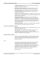
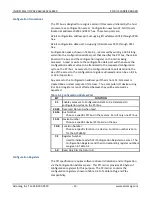
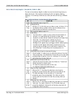
Carrier Status/Control Register - (Read/Write, P 00H) 

The Carrier Board Status Register reflects and controls functions globally on 
the carrier board.  This includes monitoring the IP Error signal, enabling, 
disabling, or monitoring IP and timeout interrupts and performing a software 
reset.   

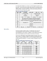
Table 3-4 Carrier Status / Control Register Bit Assignment 

BIT 

FUNCTION 

15-9 

Not Used (bits read as logic “0”) 

Write 

Only


Software Reset 

Writing a “1” to this bit causes a software reset.  Writing a “0” or 
reading this bit has no effect.  When set, the software reset 
pulse will have duration of 1 microsecond. 

Not Used (bit reads as logic “0”) 

Read 

Only 

FLASH Busy 

This bit will be “1” when a read or write to the ID FLASH is in 
progress.  On initial application of power, a FLASH read 
sequence is automatically initiated to retrieve the ID bytes from 
the FLASH.  The read sequence will take less than 5 
microseconds.  The ID bytes are stored in the ID register.  
Reading the ID register does not trigger a FLASH read sequence.   
A write to the ID register will initiate a FLASH write / read 
sequence that could take up to 3 seconds to complete.  The 
busy bit will be “1” while the write / read sequence is in 
progress. 

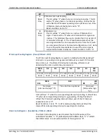
Read 

And 

Write


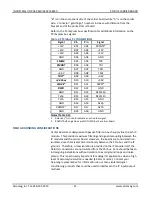
IP Module Access Time Out Interrupt Pending 

This bit will be "1" when there is an IP Module Access Time Out 
interrupt pending.  This bit will be "0" when there is no interrupt 
pending. Reset condition:  Set to "0".  Writing a “1” to this bit 
will release the pending interrupt. 

Read 

Only


IP Module Access Time Out Status 

Indicates the last IP module access has timed out.  This bit only 
reflects the last IP module access.   
“0” if last IP module access did not time out. 
“1” if last IP module access did time out. 

Read 

And 

Write


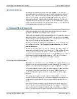
Time Out Interrupt Enable 

When set to “1”, this bit will enable the carrier board to 
generate an interrupt upon time out of an IP module access.  
The default setting or reset condition is “0” (interrupt 
generation upon time out disabled).  The interrupt service 
routine must set this bit to 0 to clear the pending interrupt 
request. 

Read 

And 

Write


IP Module Interrupt Enable 

When set to “1”, this bit will enable the generation of IP module 
interrupts.  The reset condition is “0”, (IP module interrupt 
generation disabled).  Interrupts must also be supported and 
configured in the IP modules. 

Summary of Contents for APCe8650 Series

Page 1: ...rutilized and idle equipment along with credit for buybacks and trade ins Custom engineering so your equipment works exactly as you specify Critical and expedited services Leasing Rentals Demos In sto...
Page 2: ...arrier Board USER S MANUAL ACROMAG INCORPORATED 30765 South Wixom Road P O BOX 437 Wixom MI 48393 7037 U S A Tel 248 295 0310 Fax 248 624 9234 Copyright 2016 Acromag Inc Printed in the USA Data and sp...

Page 3: ...h D 9 IP Field I O Connectors IP modules A through D 9 IP Logic Interface Connectors IP modules A through D 9 PCI Express Bus Connections 10 FIELD GROUNDING CONSIDERATIONS 11 DATA TRANSFER TIMING 12 3...

Page 4: ...Circuitry 23 PCI Interrupter 23 Power Failure Monitor 23 Power On Reset 23 Power Supply Fuses 23 Power Supply Filters 24 5 SERVICE AND REPAIR 24 SERVICE AND REPAIR ASSISTANCE 24 PRELIMINARY SERVICE PR...

Page 5: ...d makes no commitment to update or keep current the information contained in this manual No part of this manual may be copied or reproduced in any form without the prior written consent of Acromag Inc...

Page 6: ...ndard IP modules IP Modules are available from Acromag and other vendors in a wide variety of input output configurations to meet the needs of varied applications Plug And Play PCIe bus Carrier The ca...

Page 7: ...gic signals Individually Fused Power Fused 5V 12V and 12V DC power is provided A fuse is present on each supply line serving each IP module PCI Express BUS INTERFACE FEATURES Slave Module All read and...

Page 8: ...VxWorks real time operating system libraries for all Acromag IP modules and Carriers PCI I O Cards and CompactPCI I O Cards The software is implemented as a library of C functions which link with exis...

Page 9: ...results in elevated IP module and carrier board temperatures and the restricted air flow within the chassis aggravates this problem Adequate air circulation must be provided to prevent a temperature...

Page 10: ...e field I O connectors Pin assignments are defined by the IP module employed since the pins from the IP module field side correspond identically to the pin numbers of the 50 pin connectors Carrier fie...

Page 11: ...on Number Pin Description Number GND 1 GND 26 CLK 2 5V 27 Reset 3 R W 28 D00 4 IDSel 29 D01 5 DMAReq0 30 D02 6 MEMSel 31 D03 7 DMAReq1 32 D04 8 IntSel 33 D05 9 DMAck0 34 D06 10 IOSEL 35 D07 11 RESERVE...

Page 12: ...2 2 1 Asterisk is used to indicate an active low signal 2 BOLD ITALIC Logic Lines are NOT USED by the carrier board FIELD GROUNDING CONSIDERATIONS Carrier boards are designed with passive filters on...

Page 13: ...I bus memory space only The PCIe card s configuration registers are initialized by system software at power up to configure the card The PCIe carrier is a Plug and Play PCI card As a Plug and Play car...

Page 14: ...n 8 16 or 32 bit operation Any access to the Configuration address port that is not a 32 bit access is treated like a normal computer I O access Thus computer I O devices using 8 or 16 bit registers a...

Page 15: ...ter Pin Inter Line Memory Map This board occupies a 64M byte block The 64M byte block of memory consists of blocks of memory for the ID I O INT and memory spaces corresponding to four IP modules In ad...

Page 16: ...IP A ID Space 0040 007E 0081 00BF IP B ID Space IP B ID Space 0080 00BE 00C1 00FF IP C ID Space IP C ID Space 00C0 00FE 0101 013F IP D ID Space IP D ID Space 0100 013E 0141 017F Not Used1 Not Used1 01...

Page 17: ...gh the PCI Configuration Registers The addresses given in the memory map are relative to the base addresses PCIBar2 of the APCe8650 carrier as shown in Table 3 2 The addresses within each IP s own spa...

Page 18: ...sequence A write to the ID register will initiate a FLASH write read sequence that could take up to 3 seconds to complete The busy bit will be 1 while the write read sequence is in progress 5 Read An...

Page 19: ...PCIBar2 02H The IP Interrupt Pending Register is used to individually identify pending IP interrupts or a pending carrier generated interrupt as a result of IP module access time out If multiple IP in...

Page 20: ...quest via the IP Module s INTREQ1 signal An access to an interrupt select space results in the IP module serving up an interrupt vector In addition access to the interrupt space will cause some IP mod...

Page 21: ...ansmits an Assert_INTx message When using MSI interrupts a MSI interrupt message is sent The interrupt service routine determines which IP module caused the interrupt by reading the carrier interrupt...

Page 22: ...turn connect to field electronic hardware connected to the carrier board via ribbon cable The PCIe bus and IP module logic commons have a direct electrical connection i e they are not electrically iso...

Page 23: ...Module Interrupt Pending register A non volatile ID can be written to and read from a serial FLASH memory by accessing the ID register IP Logic Interface The IP logic interface is also implemented in...

Page 24: ...enabled see section 3 for programming details The PC interrupt request line assigned by the system configuration software will then be asserted The PC will respond to the asserted interrupt line by e...

Page 25: ...can be damaged unless special SMT repair and service tools are used Further Acromag has automated test equipment that thoroughly checks the performance of each board Please refer to Acromag s Service...

Page 26: ...pin male plug header AMP 173280 3 or equivalent Power Board power requirements are a function of the installed IP modules This specification lists currents for the carrier board only The carrier board...

Page 27: ...dently selected per each IP slot I O Space 16 bit and 8 bit Supports 128 byte values per IP module ID Space 16 and 8 bit Supports Type 1 32 bytes per IP consecutive odd byte addresses Also supports Ty...

Page 28: ...f whose contents are lost when power is removed Yes No Type SRAM SDRAM etc Size User Modifiable Function Process to Sanitize FPGA based RAM 540 K bits No Short term data storage Power Down Non Volatil...

Page 29: ...iagram PCIe Bus Altera Cyclone IV FPGA Tx Rx Refclk Reset Peripheral Power Connector PCIe Graphics Power Connector Power Source Select Jumper 12V 12V 12V DC DC Converter TDI TDO TCK TMS 12V 12V 5V Lev...

Page 30: ...INDUSTRIAL I O PACK SERIES APCe8650 PCI BUS CARRIER BOARD __________________________________________________________________________________________ 29 DRAWINGS...

Page 31: ...INDUSTRIAL I O PACK SERIES APCe8650 PCI BUS CARRIER BOARD __________________________________________________________________________________________ 30 B C A...

Page 32: ...ollowing table shows the revision history for this document Release Date Version EGR DOC Description of Revision 31 MAY 11 A JCL Initial Acromag release 18 OCT 13 B JCL Added Certificate of Volatility...

Page 33: ...uipment Have surplus equipment taking up shelf space We ll give it a new home Learn more Visit us at artisantg com for more info on price quotes drivers technical specifications manuals and documentat...

Reviews: