SERIES IOS-320 I/O SERVER MODULE 12-BIT HIGH DENSITY ANALOG INPUT BOARD
__________________________________________________________________________________________
- 11 -
Acromag, Inc. Tel:248-295-0310 Fax:248-624-9234 Email:solutions@acromag.com http://www.acromag.com
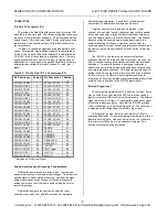
Calibration Programming Example 2
Assume that the input range is 0 to +1.25 volts. Channel 39
is connected single-ended, and corrected input channel data is
desired. From Tables 3.4 and 3.5, several calibration parameters
can be determined:
Gain = 8 (From Table 3.4)
VoltCALHI = 1.2250 volts (CAL2; From Table 3.4)
VoltCALLO = 0.6125 volts (CAL3; From Table 3.4)
Ideal_Volt_Span = 10.0000 volts (From Table 3.5)
Ideal_Zero = 0.0000 volts (From Table 3.5)
The calibration parameters (CountCALHI and CountCALLO)
remain to be determined before uncorrected input channel data
can be taken and corrected.
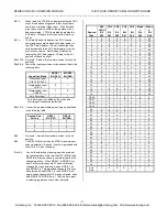
1. To prepare to measure CountCALLO, write to the Control
Register (@Base + 00H) to setup the CAL3 acquisition mode
and PGA gain = 8 by writing 00D7H. Note that "not used"
bits are set to zero.
2. Delay to allow for input settling.
3. Execute ADC Convert Command (@Base + 10H).
4. Execute Read ADC Data Command (@Base + 20H). Note
that the 12-bit data is left-justified within the 16-bit word.
5. Repeat steps 3 and 4 several times (e.g. 16) and take the
average of the ADC results. Save this number as
CountCALLO.
6. To prepare to measure CountCALHI, write to the Control
Register (@Base + 00H) to setup the CAL2 acquisition mode
and PGA gain = 8 by writing 00D6H. Note that "not used"
bits are set to zero.
7. Delay to allow for input settling.
8. Execute ADC Convert Command (@Base + 10H).
9. Execute Read ADC Data Command (@Base + 20H). Note
that the 12-bit data is left-justified within the 16-bit word.
10. Repeat steps 8 and 9 several times (e.g. 16) and take the
average of the ADC results. Save this number as
CountCALHI.
11. Calculate m = actual_slope from equation 2, since all
parameters are known.
It is now possible to correct input channel data from any input
channel using the same input range (i.e. 0 to +1.25 volts with
a PGA gain = 8). Repeat steps 1-11 periodically to re-
measure the calibration parameters (CountCALHI and
CountCALLO) as required.
12. To prepare to measure channel 39 single-ended, write to the
Control Register (@Base + 00H) to setup the single-ended
input channel 39 acquisition mode and PGA gain = 8 by
writing 02D3H. Note that "not used" bits are set to zero.
13. Delay to allow for input settling.
14. Execute ADC Convert Command (@Base + 10H).
15. Execute Read ADC Data Command (@Base + 20H). Note
that the 12-bit data is left-justified within the 16-bit word. This
data represents the uncorrected "Count_Actual" term in
equation 1. Since all parameters on the right hand side of
equation 1 are known. Calculate the calibrated value
"Corrected_Count". This is the desired, corrected value for
input channel 39.
16. Repeat steps 12-15 to re-measure channel 39's data as
desired.
Error checking should be performed on the
"Corrected_Count" value to make sure that calculated values
below 0 or above 4095 are restricted to those end points. Note
that the software calibration cannot recover signals near the end
points of each range which are clipped off due to the uncalibrated
hardware (e.g. PGA and ADC).
The maximum corrected (i.e. calibrated) error is summarized
in Table 3.6 as the worst case accuracy possible for each range.
It is the sum of error components due to ADC quantization of the
low and high calibration signals, PGA and ADC linearity error,
and the absolute errors of the recommended calibration voltages
at 25oC. Typical accuracies are significantly better.
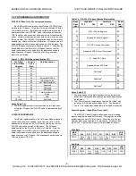
Table 3.6: Maximum Overall Calibrated Error @25 C
Input Range
(Volts)
PGA
Gain
ADC Range
(Volts)
Max Error
LSB(%
Span)
-5 to +5
1
-5 to +5
1.8 (0.044)
-2.5 to +2.5
2
"
2.1 (0.051)
-1.25 to +1.25
4
"
2.5 (0.061)
-0625 to +0.625
8
"
2.9 (0.071)
-10 to +10
1
-10 to +10
2.8 (0.069)
-5 to +5
2
"
1.8 (0.044)
-2.5 to +2.5
4
"
2.1 (0.051)
-1.25 to +1.25
8
"
2.5 (0.061)
0 to +10
1
0 to +10
3.2 (0.078)
0 to +5
2
"
2.2 (0.055)
0 to +2.5
4
"
3.1 (0.076)
0 to +1.25
8
"
5.1 (0.125)
4.0 THEORY OF OPERATION
This section describes the functionality of the IOS-320
circuitry. Refer to the IOS-320 block diagram on page 15 as you
study the following paragraphs.
ANALOG INPUTS
The field I/O interface (via the carrier board) is through
connector P2. Field analog inputs are non-isolated. This means
that the field analog return and logic common have a direct
electrical connection. Care must be taken to avoid ground loops
and excessive common mode voltage (see Section 2 for
connection recommendations). These can cause measurement
error, and with extreme abuse, circuit damage.
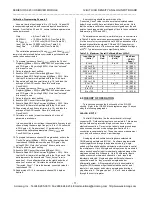
Analog inputs and calibration voltages are selected via
CMOS analog multiplexers (MUX's). A software programmable
control register contains gain, acquisition mode (e.g. single-
ended or differential) and channel selection information to control
the multiplexers. Up to 40 single-ended inputs can be monitored,
where each channel's +input is individually selected along with a
single sense lead for all channels. Up to 20 differential inputs
can be monitored, where each channel's + and - inputs are
individually selected. Single-ended and differential channels
cannot be mixed (i.e. they must all be single-ended or
differentially wired). A Programmable Gain (Instrumentation)
Amplifier (PGA) takes as input the selected channel's + and -
inputs (or + and sense) and outputs a single-ended voltage
proportional to it. The gain can be 1, 2, 4, or 8, and is selected
through the control register.

