

RTD Embedded Technologies, Inc.
|
www.rtd.com
33
ERES35105
User’s Manual
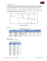
Shift Register
The shift register is used to communicate with various devices on the board. This includes digital potentiometers for setting the mode, velocity
trim, and excitation amplitude, and the excitation Programmable Waveform Generator. The commands that can be sent to the devices are
described in the following sections.
NOTE: Prior to any writes to SR_DATA_OUT or reads from SR_DATA_IN, the
Shift Register Status must be checked to make sure it is idle as
described in Section 7.3.3 on page 31.
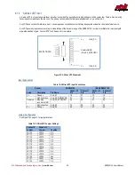
7.5.1
P
ERFORMING A
S
HIFT
R
EGISTER
C
OMMAND
To use the Shift Register, use the following steps:
1.
Read the SR_SELECT board register, and store the value.
2.
Wait until the Shift Register is idle (See Section 7.3.3 on page 31).
3.
Write to the SR_SELECT board register with the desired device.
4.
Write to the SR_DATA_OUT board register with the desired command
5.
Wait until the Shift Register is idle (See Section 7.3.3 on page 31).
6.
Read from the SR_DATA_IN register as the Read Data.
7.5.2
C
HANNEL X
M
ODE
(0
X
00
AND
0
X
02)
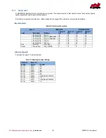
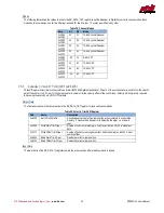
This shift register select line is connected to an Intersil ISL22424 digital potentiometer. The H pin, which corresponds to a wiper value of 0xFF,
is connected to +5V. The L pin, which corresponds to a wiper value of 0x00, is connected to -5V. For 0V, use a wiper value of 0x80.
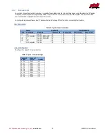
Output Data
The Table below shows the value to write to the SR_DATA_OUT register to issue various commands.
Table 27: Channel Mode Shift Register
Data
Name
Description
0x60C0
Set to Non-Volatile
All subsequent writes to the wiper position are only stored in non-volatile memory.
This should be done prior to adjusting the wiper, i.e. at board open.
0xC0XX
Write D0 Wiper
Writes to the wiper that is attached to the Resolver to Digital Converter D0 pin.
0xC1YY
Write D1 Wiper
Writes to the wiper that is attached to the Resolver to Digital Converter D1 pin.
0x8000
Read D0 Wiper
Reads from the wiper that is attached to the Resolver to Digital Converter D0 pin.
0x8100
Read D1 Wiper
Reads from the wiper that is attached to the Resolver to Digital Converter D1 pin.
Input Data
The lower 8 bits of the SR_DATA_IN register contain the wiper position after a read command is issued