PulseBlasterDDS
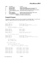
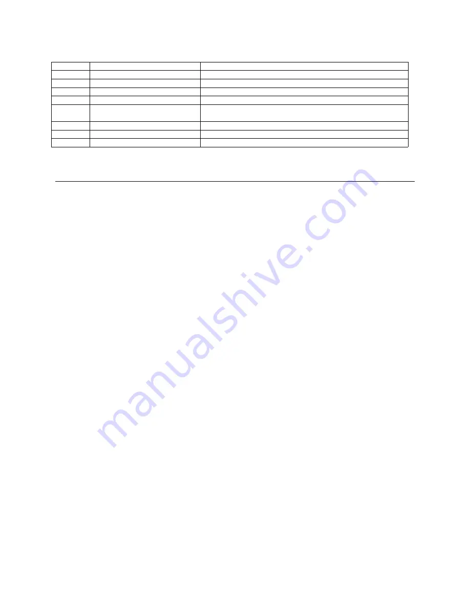
Offset
Command
Function
0
DEVICE_RESET
Stops Pulse Program
1
DEVICE_START
Starts Pulse Program (only when in initialized state)
2
SELECT_BPW
Selects number of BPW (10 for instructions)
3
SELECT_DEVICE
Using Table 2, selects internal device to be programmed
4
CLEAR_ADDRESS_COUNT
ER
Resets internal memory address counter
5
FLAG_STROBE
Strobes output clock signal to preset digital outputs
6
DATA_TRANSFER
Data to be written to internal device
7
PROGRAMMING_FINISHED
Sets device in initialized state
Table A1.2:
Port Offset Command Functions
Example Program
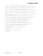
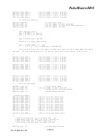
The following is an example of the output sequence to program the PulseBlasterDDS. You must use the
PBD03PC_outp(addr, data) function from the provided DLL in order to use this method.
//
Initialization:
PBD03PC_outp(0,0);
//(Issue device reset)
PBD03PC_outp(2,4);
//(Select number of bytes per word)
PBD03PC_outp(3,0xFF);
//(Select device to program (Flag initial values))
PBD03PC_outp(4,0);
//(Reset address counter)
//
Set initial flag values
//
Values for this example are "0x000000f0"
PBD03PC_outp(6,0);
//(Data transfer)
PBD03PC_outp(6,0);
//(Data transfer)
PBD03PC_outp(6,0);
//(Data transfer)
PBD03PC_outp(6,0xF0);
//(Data transfer)
PBD03PC_outp(5,0);
//(Clock data into external buffer)
PBD03PC_outp(5,0);
//(Return clock signal to low)
//
Set up DDS frequency registers
PBD03PC_outp(0,0);
//(Issue device reset)
PBD03PC_outp(2,4);
//(Select number of bytes per word)
PBD03PC_outp(3,1);
//(Select device to program (DDS Frequency Registers))
PBD03PC_outp(4,0);
//(Reset address counter)
/*
DDS Register Values
Reg0 = 051EB852 (1 MHz)
Reg1 = 0A3D70A4 (2 MHz)
.
.
Reg15 = 147AE148 (4 MHz)
Formula for finding these values:
REG0 = DESIRED_FREQUENCY * 2
32
/ PBDDS_CLOCK
= 1 MHz * 2
32
/ 50 MHz = 858993459.2 = 0x051EB852
*/
PBD03PC_outp(6,0x05);
//(Data Transfer - Byte 3 of Reg0)
PBD03PC_outp(6,0x1E);
//(Data Transfer - Byte 2 of Reg0)
PBD03PC_outp(6,0xB8);
//(Data Transfer - Byte 1 of Reg0)
PBD03PC_outp(6,0x52);
//(Data Transfer - Byte 0 of Reg0)
PBD03PC_outp(6,0x05);
//(Data Transfer - Byte 3 of Reg1)
PBD03PC_outp(6,0x3D);
//(Data Transfer – Byte 2 of Reg1)
PBD03PC_outp(6,0x70);
//(Data Transfer - Byte 1 of Reg1)
PBD03PC_outp(6,0xA4);
//(Data Transfer - Byte 0 of Reg1)
.
.
9/20/200524
www.spincore.com


