PulseBlasterDDS
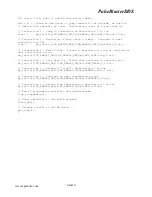
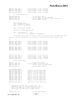
PBD03PC_outp(6,0x14);
//(Data Transfer - Byte 3 of Reg15)
PBD03PC_outp(6,0x7A);
//(Data Transfer - Byte 2 of Reg15)
PBD03PC_outp(6,0xE1);
//(Data Transfer - Byte 1 of Reg15)
PBD03PC_outp(6,0x48);
//(Data Transfer - Byte 0 of Reg15)
//
Set up phase registers
PBD03PC_outp(0x0);
//(Issue device reset)
PBD03PC_outp(2,4);
//(Select number of bytes per word)
PBD03PC_outp(3,2);
//(Select device to program (TX Phase Registers))
PBD03PC_outp(4,0);
//(Reset address counter)
/*
Phase Register Values
Reg0 = 093E93E9 (13 degrees)
Reg1 = 40000000 (90 degrees)
.
.
Reg15 = E0000000(315 degrees)
Formula for finding these values:
REG0 = DESIRED_PHASE * 2
32
/ 360
= 13 * 2
32
/ 360 = 155096041.24
≈
0x093E93E9
* Note that only the top 3 hex digits (0x093) are actually used in programming the phase
register. The other digits must still be sent so that the DDS word remains 32 bits long.
*/
PBD03PC_outp(6,0x09);
//(Data Transfer - Byte 3 of Reg0)
PBD03PC_outp(6,0x3E);
//(Data Transfer - Byte 2 of Reg0)
PBD03PC_outp(6,0x93);
//(Data Transfer - Byte 1 of Reg0)
PBD03PC_outp(6,0xE9);
//(Data Transfer - Byte 0 of Reg0)
PBD03PC_outp(6,0x40);
//(Data Transfer - Byte 3 of Reg1)
PBD03PC_outp(6,0x00);
//(Data Transfer - Byte 2 of Reg1)
PBD03PC_outp(6,0x00);
//(Data Transfer - Byte 1 of Reg1)
PBD03PC_outp(6,0x00);
//(Data Transfer - Byte 0 of Reg1)
.
.
PBD03PC_outp(6,0xE0);
//(Data Transfer - Byte 3 of Reg15)
PBD03PC_outp(6,0x00);
//(Data Transfer - Byte 2 of Reg15)
PBD03PC_outp(6,0x00);
//(Data Transfer - Byte 1 of Reg15)
PBD03PC_outp(6,0x00);
//(Data Transfer - Byte 0 of Reg15)
//
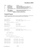
Pulse Program Setup
PBD03PC_outp(0,0);
//(Issue Device Reset)
PBD03PC_outp(2,10);
//(Select number of bytes per word)
PBD03PC_outp(3,0);
//(Select device to program (RAM))
PBD03PC_outp(4,0);
//(Reset address counter)
//Send pulse program
PBD03PC_outp(6,0x18);
//(Byte 9 of first instruction)
PBD03PC_outp(6,0xFF);
//(Byte 8 of first instruction)
PBD03PC_outp(6,0xFF);
//(Byte 7 of first instruction)
PBD03PC_outp(6,0x00);
//(Byte 6 of first instruction)
PBD03PC_outp(6,0x00);
//(Byte 5 of first instruction)
PBD03PC_outp(6,0x00);
//(Byte 4 of first instruction)
PBD03PC_outp(6,0x00);
//(Byte 3 of first instruction)
PBD03PC_outp(6,0x00);
//(Byte 2 of first instruction)
PBD03PC_outp(6,0x00);
//(Byte 1 of first instruction)
PBD03PC_outp(6,0x07);
//(Byte 0 of first instruction)
PBD03PC_outp(6,0xXX);
//(Byte 9 of second instruction)
/*
Continue this process for all instructions. The
explanation of how to create the 80 bit instruction
words is included above. When finished with all
instructions, continue with the sequence below.
*/
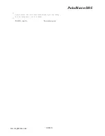
PBD03PC_outp(7,0);
//(Programming Finished)
9/20/200525
www.spincore.com


