background image

FPGA Registers 

              EPU-4562 Programmer’s Reference Manual 


11 


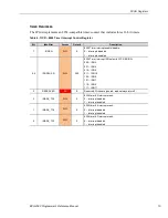
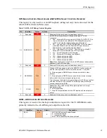
Table 7: TISR – 8254 Timer Interrupt Status Register 

Bit 

Identifier 

Access 

Default 

Description 

RESERVED 

RO 

Reserved. Writes are ignored; reads always return 0. 

RESERVED 

RO 

Reserved. Writes are ignored; reads always return 0. 

RESERVED 

RO 

Reserved. Writes are ignored; reads always return 0. 

RESERVED 

RO 

Reserved. Writes are ignored; reads always return 0. 

RESERVED 

RO 

Reserved. Writes are ignored; reads always return 0. 

ISTAT_TC5 

RW/C 

N/A 

Status for the 8254 Timer #5 output (terminal count) interrupt 
when read. This bit is read-status and a write-1-to-clear. 

0 – Timer output (terminal count) has not transitioned from 0 to 
a 1 level 

1 – Timer output (terminal count) has transitioned from a 0 to a 
1 level 

ISTAT_TC4 

RW/C 

N/A 

Status for the 8254 Timer #4 output (terminal count) interrupt 
when read. This bit is read-status and a write-1-to-clear. 

0 – Timer output (terminal count) has not transitioned from 0 to 
a 1 level 

1 – Timer output (terminal count) has transitioned from a 0 to a 
1 level 

ISTAT_TC3 

RW/C 

N/A 

Status for the 8254 Timer #3 output (terminal count) interrupt 
when read. This bit is read-status and a write-1-to-clear. 

0 – Timer output (terminal count) has not transitioned from 0 to 
a 1 level 

1 – Timer output (terminal count) has transitioned from a 0 to a 
1 level 


Summary of Contents for Blackbird VL-EPU4562

Page 1: ...ogrammer s Reference Manual REV May 2018 Blackbird VL EPU 4562 Intel Core based Embedded Processing Unit with SATA Dual Ethernet USB Digital I O Serial Video Mini PCIe Sockets SPX Trusted Platform Module ...

Page 2: ... VersaLogic makes no representations or warranties with respect to this product and specifically disclaims any implied warranties of merchantability or fitness for any particular purpose VersaLogic reserves the right to revise this product and associated documentation at any time without obligation to notify anyone of such changes PC 104 PC 104 Plus and the PC 104 logo are trademarks of the PC 104...

Page 3: ... information and resources for this product including Reference Manual PDF format Operating system information and software drivers Data sheets and manufacturers links for chips used in this product BIOS information and upgrades Utility routines and benchmark software The VersaTech KnowledgeBase is an invaluable resource for resolving technical issues with your VersaLogic product VersaTech Knowled...

Page 4: ... register is used as the interrupt control status register for the TI ADS8668A and is primarily related to the ALARM signal output from the A D 21 FANCON Fan Control Register 31 FANTACHLS FANTACHMS FANTACH Status Registers 32 Programming Information for Hardware Interfaces 41 Watchdog Timer 41 Programmable LED 41 Processor WAKE Capabilities 42 Tables Table 1 FPGA I O Map 3 Table 2 FPGA Register Ma...

Page 5: ...OISTAT1 Digital I O 8 1 Interrupt Mask Register 24 Table 29 DIOISTAT2 Digital I O 16 9 Interrupt Mask Register 25 Table 30 DIOCR Digital I O Control Register 25 Table 31 AUXDIR AUX GPIO Direction Control Register 26 Table 32 AUXPOL AUX GPIO Polarity Control Register 26 Table 33 AUXOUT AUX GPIO Output Control Register 27 Table 34 AUXIN AUX GPIO Input Status Register 27 Table 35 AUXICR AUX GPIO Inte...

Page 6: ...ith the VL EPU 4562 Related Documents The following documents are available on the EPU 4562 Product Support Web Page VL EPU 4562 Hardware Reference Manual provides information on the board s hardware features including connectors and all interfaces Operating System compatibility and software package downloads are available at the VersaLogic Software Support page 1 ...

Page 7: ...l stick and are cleared by a write one to a status register bit The 16550 UART interrupts behave as defined for the 16550 registers and are a pass through to the LPC SERIRQ Per the VersaAPI standard anytime an interrupt on the SERIRQ is enabled the slot becomes active All interrupts in the SERIRQ are high true so when the slot becomes active the slot will be low when there is no interrupt and high...

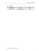
Page 8: ...System Resources and Maps EPU 4562 Programmer s Reference Manual 3 Table 1 FPGA I O Map Address Range Device Size 0x1C80 0x1CBB FPGA registers 60 bytes 0x1CBC 0x1CBF 8254 timer address registers 4 bytes ...

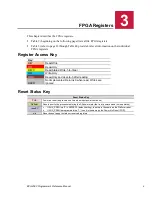
Page 9: ...WO Write Only ROC Read Only and clear to 0 after reading RSVD Not implemented Returns 0 when read Writes are ignored Reset Status Key Reset Status Key POR Power on reset only resets one time when input power comes on Platform Resets prior to the processor entering the S0 power state that is at power on and in sleep states resetSX If AUX_PSEN is a 0 in MISCSR1 default setting then this is the same ...

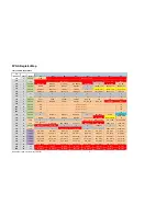
Page 10: ... DACLDA C8F F Platform IRQEN IRQSEL2 IRQSEL1 IRQSEL0 ADC_RESET IN_ALARM ISTAT_ALARM IMASK_ALAR M C90 10 POR 0 0 0 0 MINI3_PSDIS MINI2_PSDIS AUX_PSEN MINI1_PSDIS C91 11 POR USB_HUBMOD E W_DISABLE USB_HUBDIS ETH0_OFF USB2_OC2 USB2_OC1 USB2_DIS2 USB2_DIS1 C92 12 Platform PROCHOT LVDS_OC 0 0 0 PBRESET 0 TPM_PP C93 13 POR 0 0 USB3_OC2 USB3_OC1 0 0 USB3_DIS2 USB3_DIS1 C94 14 resetSX DIR_DIO8 DIR_DIO7 DI...

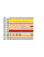
Page 11: ...PIO3 IMASK_GPIO2 IMASK_GPIO1 CA6 26 Platform ISTAT_GPIO8 ISTAT_GPIO7 ISTAT_GPIO6 ISTAT_GPIO5 ISTAT_GPIO4 ISTAT_GPIO3 ISTAT_GPIO2 ISTAT_GPIO1 CA7 27 resetSX MODE_GPIO8 MODE_GPIO7 MODE_GPIO6 MODE_GPIO5 MODE_GPIO4 MODE_GPIO3 MODE_GPIO2 MODE_GPIO1 CA8 28 Platform IRQEN IRQSEL2 IRQSEL1 IRQSEL0 0 RESET_EN WDT_EN WDT_STAT CA9 29 Platform msb lsb CAA 2A Platform 0 0 0 0 COM4_MODE COM3_MODE COM2_MODE COM1_...

Page 12: ...s EPU 4562 Programmer s Reference Manual 7 I O Address Offset Reset D7 D6 D5 D4 D3 D2 D1 D0 CBB 3B n a 0 0 0 0 0 0 0 0 CBC 3C Platform msb lsb CBD 3D Platform msb lsb CBE 3E Platform msb lsb CBF 3F Platform msb lsb ...

Page 13: ... is off default 1 LED is on 6 0 PRODUCT_CODE RO 0010011 Product Code for the EPU 4562 0x13 Table 4 PSR Product Status Register Bit Identifier Access Default Description 7 3 REV_LEVEL 4 0 RO N A Revision level of the PLD incremented every FPGA release 0 Indicates production release revision level when BETA status bit bit 0 is set to 0 1 Indicates development release revision level when BETA status ...

Page 14: ...ected the one on the COM Module 1 Backup BIOS selected the one on the base board Note If the external BIOS configuration jumper is set to Backup then setting this will not have any affect The jumper must not be installed to use this selection mode Must have BIOS_OR set to a 1 for this to have any affect 4 LED_DEBUG R W 0 Debug LED controls the yellow LED 0 LED is off and follows its primary functi...

Page 15: ...terrupts disabled 1 Interrupts enabled 6 4 IRQSEL 2 0 R W 000 8254 Timer interrupt IRQ select in LPC SERIRQ 000 IRQ3 001 IRQ4 010 IRQ5 011 IRQ10 100 IRQ6 101 IRQ7 110 IRQ9 111 IRQ11 3 RESERVED RO 0 Reserved Writes are ignored reads always return 0 2 IMASK_TC5 R W 0 8254 timer 5 interrupt mask 0 Interrupt disabled 1 Interrupt enabled 1 IMASK_TC4 R W 0 8254 timer 4 interrupt mask 0 Interrupt disable...

Page 16: ...rupt when read This bit is read status and a write 1 to clear 0 Timer output terminal count has not transitioned from 0 to a 1 level 1 Timer output terminal count has transitioned from a 0 to a 1 level 1 ISTAT_TC4 RW C N A Status for the 8254 Timer 4 output terminal count interrupt when read This bit is read status and a write 1 to clear 0 Timer output terminal count has not transitioned from 0 to...
Page 17: ... Gate on signal GCTC3 is enabled Always set to 0 when configuring timer modes except when TMRFULL is 0 and then it should be set to 1 and not changed unless using internal clocking 4 TM45MODE R W 0 Mode to set timers 4 and 5 in 0 Timer 4 and 5 form one 32 bit timer controlled by timer 1 signals 1 Timer 4 and Timer 5 are separate 16 bit timers with their own control signals Almost always used in 32...

Page 18: ...te if they support any Wake events 1 Minicard 3 3 V power will be turned off when not in S0 in sleep modes The Minicard 3 3 V power switch is controlled by the OR of the S0 power control signal and the inverse of MINI2_PSDIS 1 AUX_PSEN R W 0 CBR 4005B 8xGPIO sometimes called AUX GPIOs I O Power Enable 0 The GPIO pullups will be powered down in sleep modes only power in S0 1 The GPIO pullups will n...

Page 19: ...ways on power well of the FPGA It holds its state during sleep modes and can only be reset by a power cycle It is primarily used for control signals for the always powered Ethernet controllers and the USB hubs This register is only reset by the main power on reset since it must maintain its state in sleep modes for example S3 ...

Page 20: ...s Ethernet controller 0 controls the ETH_OFF input to the I210 IT 0 Ethernet controller is enabled On 1 Ethernet controller is disabled Off 3 USB2_OC2 RO N A Overcurrent Status from the USB 2 0 port 2 3 VBUS power switches This signal also passed to the fourth USB_6_7_OC input on the COM Express connector 0 VBUS power switch is not in overcurrent either OK or disabled 1 VBUS power switch is in ove...

Page 21: ... THERMTRIP is asserted 6 LVDS_OC RO N A The overcurrent status from the LVDS panel power switch If this is ever asserted the LVDS panel enable signal must be de asserted and then asserted to unlatch the power fault condition on the power switch 0 LVDS Overcurrent is not asserted 1 LVDS Overcurrent is asserted 3 5 Reserved RO N A Reads the overcurrent status for the USB paddleboard power switches t...

Page 22: ...wer switch is in an overcurrent shutdown state and must be restarted 4 USB3_OC1 RO N A The status of the overcurrent signal on VBUS power switch for first USB 3 0 Port 1 This signal also passed to the first USB_0_1_OC input on the COM Express connector 0 USB 3 0 VBUS power switch is operating normally or it is disabled 1 USB 3 0 VBUS power switch is in an overcurrent shutdown state and must be res...

Page 23: ...ge on which valid data will be read 0 Data is read on rising edge 1 Data is read on falling edge 5 4 SPILEN 1 0 R W 00 Determines the SPI frame length This selection works in manual and auto slave select modes 00 8 bit 01 16 bit 10 24 bit 11 32 bit 3 MAN_SS R W 0 Determines whether the slave select lines are asserted through the user software or are automatically asserted by a write to SPIDATA3 0 ...

Page 24: ...z 4 3 HW_IRQ_EN R W 0 The SPX interrupt is not connected on this product always de asserted This enables the selected IRQ to be activated by a SPI device that is configured to use its interrupt capability 0 IRQs are disabled for SPI operations 1 The IRQ can be asserted 2 LSBIT_1ST R W 0 Controls the SPI shift direction from the SPIDATA x registers 0 Data is left shifted MSB first 1 Data is right s...

Page 25: ...select to begin an SPI bus transaction Data is sent according to the LSBIT_1ST setting When LSBIT_1ST 0 the MSbit of SPIDATA3 is sent first and received data will be shifted in the LSbit of the selected frame size determined by SPILEN1 and SPILEN0 When LSBIT_1ST 1 the LSbit of the selected frame size is sent first and the received data will be shifted in the MSbit of SPIDATA3 SPIDATA0 Least Signif...

Page 26: ...hen the Minicard uses PCIe the SATA channel automatically switches to the SATA connector 3 Reserved RO 0 Reserved Writes are ignored reads always return 0 2 SERIRQEN R W 0 When an IRQ is assigned a slot in the SERIRQ it will drive the slot with the interrupt state but this bit must be set to a 1 to do that 0 Slots assigned to SERIRQ are not driven available for other devices 1 Slots assigned to SE...

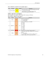
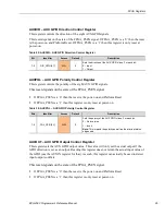
Page 27: ...t status Writing a 1 will clear the interrupt status This bit is set to a 1 on a transition from low to high of the ADC ALARM signal alarm assertion 0 IMASK_ALARM RW 0 ADC ALARM Interrupt Mask 0 Interrupt disabled 1 Interrupt enabled DIODIRx x 1 2 Digital I O Direction Control Registers These two registers control the directions of the 16 digital I O signals This reset depends on the state of the ...

Page 28: ...ster does not return the actual input value of the DIO use the DIOIN register for that As such this register can actually be used to detect input output conflicts This reset depends on the state of the FPGA_PSEN signal If FPGA_PSEN is a 0 then the reset is the power on and Platform Reset If FPGA_PSEN is a 1 then this register is only reset at power on Table 20 DIOOUT1 Digital I O 8 1 Output Contro...

Page 29: ...e the interrupt mask registers for the digital IOs The reset type is Platform Reset because interrupts always have to be setup after exiting sleep states Table 24 DIOIMASK1 Digital I O 8 1 Interrupt Mask Register Bits Identifier Access Default Description 7 0 IMASK_DIO 8 1 R W 0 Digital I O 8 1 interrupt mask For each bit 0 Interrupt disabled 1 Interrupt enabled Table 25 DIOIMASK2 Digital I O 16 9...

Page 30: ...rated for the 16 digital I Os Reset type is Platform Table 28 DIOCR Digital I O Control Register Bits Identifier Access Default Description 7 IRQEN R W 0 DIO interrupt enable disable 0 Interrupts disabled 1 Interrupts enabled 6 4 IRQSEL 2 0 R W 000 DIO interrupt IRQ select in LPC SERIRQ 000 IRQ3 001 IRQ4 010 IRQ5 011 IRQ10 100 IRQ6 101 IRQ7 110 IRQ9 111 IRQ11 3 1 RESERVED RO 000 Reserved Writes ar...

Page 31: ...a 0 then the reset is the power on and Platform Reset If FPGA_PSEN is a 1 then this register is only reset at power on Table 30 AUXPOL AUX GPIO Polarity Control Register Bits Identifier Access Default Description 7 0 POL_GPIO 8 1 R W 0 Sets the polarity of the AUX GPIOx lines For each bit 0 No inversion 1 Invert Note This impacts the polarity as well as the interrupt status edge used AUXOUT AUX GP...

Page 32: ...h bit 0 Input de asserted if polarity not inverted asserted if polarity inverted 1 Input asserted if polarity not inverted de asserted if polarity inverted AUXIMASK AUX GPIO Interrupt Mask Register This is the interrupt mask register for the AUX GPIOs and the interrupt enable selection The reset type is Platform Reset because interrupts always have to be setup after exiting sleep states Table 33 A...

Page 33: ...e the GPIO will be the FPGA watchdog timer trigger output that signals external equipment that the watchdog fired The GPIO input status can still be read Default is low true Setting GPIO polarity to 1 makes it high true 2 MODE_GPIO3 R W 0 GPIO3 mode 0 GPIO I O 1 WAKE input only In this mode the GPIO is passed through to the PCI_WAKE signal Default is low true Setting GPIO polarity to 1 makes it hi...

Page 34: ...10 IRQ9 111 IRQ11 3 Reserved RO 0 Reserved Writes are ignored reads always return 0 2 RESET_EN R W 0 Enable the Watchdog to assert the push button reset if it fires 0 Watchdog will not reset the board 1 Board will be reset if the Watchdog fires 1 WDT_EN R W 0 Watchdog Enable 0 Watchdog is disabled 1 Watchdog is enabled Note The WDT_VAL register must be set before enabling 0 WDT_STAT RO 0 Watchdog ...

Page 35: ...e 37 WDT_VAL Watchdog Control Register Bits Identifier Access Default Description 7 0 WDT_VAL 7 0 R W 0x00 Number of seconds before the Watchdog fires By default it is set to zero which results in an immediate watchdog if WDT_EN is set to a 1 XCVRMODE COM Transceiver Mode Register Sets the RS232 vs RS422 485 mode on the COM port transceivers These drive the UART_SEL signals from the FPGA to the tr...

Page 36: ...to default by the platform reset signal The fan is always turned off in sleep modes On other products the FPGA controlled the fan and monitored fan speed The FPGA on this products does that as well but the COM Module can also control the fan either on off or PWM and monitor the fan speed The FPGA currently only allows the fan to be turned on or off no PWM since that requires interleaved fan speed ...

Page 37: ...control only applies when COM_MODE is a 0 FPGA controls fan on off FANTACHLS FANTACHMS FANTACH STATUS REGISTERS The FPGA fan tach readings are always available and do not depend on either COM_MODE or the FAN_OFF settings The number of fan tach output samples over a 1 second sampling period The value is always valid after the fan speed stabilizes and is updated every 1 sec after a delay of 1 sec Cu...

Page 38: ...s Table 42 FANTACHMS FANTACH Status Register MS Bits Bits Identifier Access Default Description 7 0 FANTACH 15 8 RO N A LS 8 bits of FANTACH read this first since it latches the value for the MS 8 bits Note The FANTACHLS register must be read first It will latch a copy of the MS bits so that when FANTACHMS is read it is based on the same 16 bit value This assumes that a 16 bit word read on the LPC...

Page 39: ...le 43 UART1CR UART1 Control Register COM1 Bits Identifier Access Default Description 7 IRQEN R W 0 UART interrupt enable disable 0 Interrupts disabled 1 Interrupts enabled 6 4 IRQSEL 2 0 R W 001 UART interrupt IRQ select in LPC SERIRQ 000 IRQ3 001 IRQ4 COM1 Default 010 IRQ5 011 IRQ10 100 IRQ6 101 IRQ7 110 IRQ9 111 IRQ11 3 0 UART1_BASE 3 0 R W 0000 UART Base Address 0000 3F8h COM1 Default 0001 2F8h...

Page 40: ... interrupt enable disable 0 Interrupts disabled 1 Interrupts enabled 6 4 IRQSEL 2 0 R W 000 UART interrupt IRQ select in LPC SERIRQ 000 IRQ3 COM2 Default 001 IRQ4 010 IRQ5 011 IRQ10 100 IRQ6 101 IRQ7 110 IRQ9 111 IRQ11 3 0 UART2_BASE 3 0 R W 0001 UART Base Address 0000 3F8h 0001 2F8h COM2 Default 0010 3E8h 0011 2E8h 0100 200h 0101 208h 0110 220h 0111 228h 1000 238h 1001 338h 1010 1111 These values...

Page 41: ... interrupt enable disable 0 Interrupts disabled 1 Interrupts enabled 6 4 IRQSEL 2 0 R W 101 UART interrupt IRQ select in LPC SERIRQ 000 IRQ3 001 IRQ4 010 IRQ5 011 IRQ10 100 IRQ6 101 IRQ7 COM3 Default 110 IRQ9 111 IRQ11 3 0 UART2_BASE 3 0 R W 0010 UART Base Address 0000 3F8h 0001 2F8h 0010 3E8h COM3 Default 0011 2E8h 0100 200h 0101 208h 0110 220h 0111 228h 1000 238h 1001 338h 1010 1111 These values...

Page 42: ... interrupt enable disable 0 Interrupts disabled 1 Interrupts enabled 6 4 IRQSEL 2 0 R W 011 UART interrupt IRQ select in LPC SERIRQ 000 IRQ3 001 IRQ4 010 IRQ5 011 IRQ10 COM4 Default 100 IRQ6 101 IRQ7 110 IRQ9 111 IRQ11 3 0 UART2_BASE 3 0 R W 0011 UART Base Address 0000 3F8h 0001 2F8h 0010 3E8h 0011 2E8h COM4 Default 0100 200h 0101 208h 0110 220h 0111 228h 1000 238h 1001 338h 1010 1111 These values...

Page 43: ... 485 and Automatic Direction Control is disabled e g UART1_485ADC set to 0 then the UART is in Manual Direction Control mode and the transceiver Tx output enable is controlled by software using the RTS bit in the UART Modem Control Register RTS 0 Transceiver Tx output is enabled RTS 1 Transceiver Tx output is disabled i e tri stated Warning Terminal software expecting an RS 232 port may set RTS to...

Page 44: ...MODE register must also be set to a 1 4 UART1_485ADC R W 0 COM1 RS 485 Automatic Direction Control 0 Disabled 1 Enabled Note Only enable in RS 485 mode The COM1_MODE in XCVRMODE register must also be set to a 1 3 UART4_EN R W 0 UART 4 Output Enable 0 Tx and RTS outputs are disabled 1 Tx and RTS outputs are enabled Note If disabled the UART I O space is freed up 2 UART3_EN R W 0 UART 3 Output Enabl...

Page 45: ...he 16x UART clock This bit must be set to use rates above 115 200 and may require custom software Reset type is Platform Note The values shown are for the default BIOS configuration Table 48 UARTMODE2 UART MODE Register 2 Bits Identifier Access Default Description 7 1 Reserved RO 0000000 Reserved Writes are ignored reads always return 0 0 FAST_MODE R W 0 Sets how the baud rate divisor for the 1655...

Page 46: ... the actual timeout is WDT_VAL seconds with a 1 second to 0 second error band The Watchdog control status register s have bits for the following Watchdog enable disable disabled by default Watchdog timeout status This is cleared when the Watchdog is disabled or when a new value is written to WDT_VAL Writing WDT_VAL would be the interrupt acknowledge Watchdog interrupt IRQ select from the same list...

Page 47: ...PCIE_WAKE signal to the CPU module I210 Ethernet controller Minicard 1 WAKE signal Minicard 2 WAKE signal FPGA via a secondary function on one of the 8x GPIOs The following USB devices can wake up the processor using the in band SUSPEND protocol On board USB 3 0 port Any of the four USB Ports on the CBR 4005B paddleboard Minicard 1 USB port Minicard 2 USB port End of document ...

Reviews: