FPGA Registers
EPU-4562 Programmer’s Reference Manual
13
M
ISCELLANEOUS
FPGA
R
EGISTERS
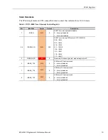
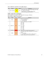
MISCSR1 – Miscellaneous Control Register #1
This is a register in the always-on power well of the FPGA. It holds its state during sleep modes
and can only be reset by a power cycle. This is a placeholder register for features like pushing the
power-button and also for software initiated resets should those be needed.
Reset: This register is only reset by the main power-on reset since it must maintain its state in
Sleep modes (for example, S3).
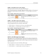
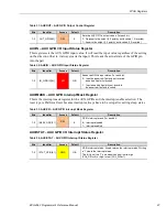
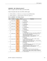
Table 9: MISCSR1 – Misc. Control Register #1
Bits
Identifier
Access
Default
Description
7-4
Reserved
RO
00000
Reserved. Writes are ignored; reads always return 0.
2
MINI2_PSDIS
R/W
0
Minicard #2 3.3 V power disable
0 – Minicard 3.3 V power stays on always (this is normally how
minicards operate if they support any Wake events)
1 – Minicard 3.3 V power will be turned off when not in S0 (in sleep
modes).
The Minicard 3.3 V power switch is controlled by the “OR” of the S0
power control signal and the inverse of MINI2_PSDIS.
1
AUX_PSEN
R/W
0
CBR-4005B 8xGPIO (sometimes called “AUX” GPIOs) I/O Power
Enable
0 – The GPIO pullups will be powered down in sleep modes (only
power in S0)
1 – The GPIO pullups will not be powered down in sleep modes
and the configuration will remain.
This power is used for both the GPIO pullup voltage and for the
3.3V power on Pin 37 of the User Interface connector J2.
Note:
Some register resets are conditional on the state of
AUX_PSEN
0
MINI1_PSDIS
R/W
0
Minicard #1 3.3 V power disable
0 – Minicard 3.3 V power stays on always (this is normally how
minicards operate if they support any Wake events)
1 – Minicard 3.3 V power will be turned off when not in S0 (in sleep
modes).
The Minicard 3.3 V power switch is controlled by the “OR” of the S0
power control signal and the inverse of MINI1_PSDIS.

