FPGA Registers
EPU-4562 Programmer’s Reference Manual
27
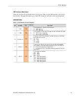
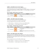
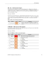
Table 31: AUXOUT – AUX GPIO Output Control Register
Bits
Identifier
Access
Default
Description
7-0
OUT_GPIO[8:1]
R/W
0
Sets the AUX GPIOx output values. For each bit:
0 – De-asserts the output (0 if polarity not-inverted, 1 if inverted)
1 – Asserts the output (1 if polarity not-inverted, 0 if inverted)
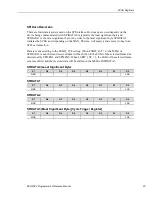
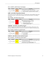
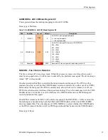
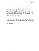
AUXIN – AUX GPIO I/O Input Status Register
This register sets the AUX GPIO input value. It will read the input value regardless of the setting
on the direction (that is, it always reads the input). This reads the actual state of the GPIO pin
into the part.
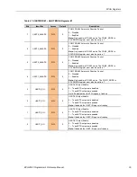
Table 32: AUXIN – AUX GPIO Input Status Register
Bits
Identifier
Access
Default
Description
7-0
IN_GPIOIO[8:1]
RO
N/A
Reads the GPIOx input status. For each bit:
0 – Input de-asserted if polarity not-inverted;
asserted if polarity inverted
1 Input asserted if polarity not-inverted;
de-asserted if polarity inverted
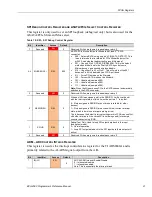
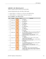
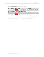
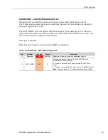
AUXIMASK – AUX GPIO Interrupt Mask Register
This is the interrupt mask register for the AUX GPIOs and the interrupt enable selection. The
reset type is Platform Reset because interrupts always have to be setup after exiting sleep states.
Table 33: AUXICR – AUX GPIO Interrupt Mask Register
Bits
Identifier
Access
Default
Description
7-0
IMASK_GPIO[8:1]
R/W
0
GPIOx interrupt mask. For each bit:
0 – Interrupt disabled
1 – Interrupt enabled
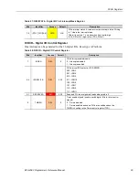
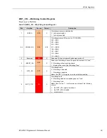
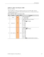
AUXISTAT – AUX GPIO I/O Interrupt Status Register
Table 34: AUXISTAT – AUX GPIO Interrupt Status Register
Bits
Identifier
Access
Default
Description
7-0
ISTAT_GPIO[8:1]
RW/C
N/A
GPIOx interrupt status. A read returns the interrupt status. Writing
a ‘1’ clears the interrupt status.
This bit is set to a ‘1’ on a transition from low-to-high
(POL_DIOx=0) or high-to-low (POL_DIOx=1).


