background image


Embedded Solutions


Page 21 of 37


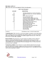
BIS3_SDLC_CNTL7-0 

[$B0, A0, 90, 80, 70, 60, 50, 40] BiSerial III SDLC Control Registers 


SDLC Control Registers 


DATA BIT 

DESCRIPTION 


31 

Idle Detected/Clear (see note after description) 


30 

Abort Detected/Clear (see note after description) 


29-25 

spare 


24 

SDLC Internal Clock Select 


23 

Send an Abort (write only) 


22 

Load Transmit End Address (write only) 


21 

Load Transmit Start Address/SDLC Done 


20 

Load Receive Start Address/SDLC Sending Data  


19 

SDLC Idle After Frame Done 


18-8 

Address Input/ Receive End Address 


Repeated Flags Share Zero 


Received Abort Interrupt Enable 


Receive Interrupt Enable 


Transmit Frame Done Interrupt Enable 


Transmit Interrupt Enable 


Transmit Clear Enable 


Receive Enable 


Transmit Enable 


FIGURE 15 

PMC BISERIAL-III SDLC CONTROL REGISTERS 


Transmit Enable

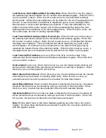
: When this bit is a one the transmitter is enabled to send data starting 

with the address stored in the transmitter start-address register and continuing until the 
data at the address in the transmitter end-address register has been sent.  When this 
bit is a zero the transmitter is disabled.


Receive Enable

: When this bit is a one the receiver is enabled to receive data and 

store it in the dual-port RAM starting with the address stored in the receiver start-
address register if it is the first message since the receiver was enabled, or in the next 
16-bit address after the end-address of the last message if it is not.  When this bit is a 
zero the receiver is disabled.


Transmit Clear Enable

: When this bit is a one the transmit enable bit will be cleared 

when the transmitted message completes and there is not another message pending.  
When this bit is a zero the transmitter will remain enabled, but no more data will be sent 
until a new end address is loaded. 

Summary of Contents for PMC-BiSerial-III SDLC

Page 1: ...Cruz CA 95060 831 457 8891 Fax 831 457 4793 www dyneng com sales dyneng com Est 1988 User Manual PMC BiSerial III SDLC 8 channel SDLC Interface PMC Module Revision A1 Corresponding Hardware Revision E 10 2005 0205 Corresponding Firmware Revision B ...

Page 2: ... Furthermore Dynamic Engineering assumes no liability arising out of the application or use of the device described herein The electronic equipment described herein generates uses and can radiate radio frequency energy Operation of this equipment in a residential area is likely to cause radio interference in which case the user at his own expense will be required to take whatever measures may be r...

Page 3: ... BIS3_IO_TERM 16 BIS3_IO_MUX 17 BIS3_IO_UCNTL 17 BIS3_IO_RDBK 18 BIS3_IO_RDBKUPR 18 BIS3_SWITCH 19 BIS3_PLL_CMD PLL_RDBK 20 BIS3_SDLC_CNTL7 0 21 BIS3_INT_STAT 24 BIS3_I2OAR 24 Mode Resource Mapping 25 Channel I O Line Mapping 26 Interrupts 27 Loop back 28 PMC PCI PN1 INTERFACE PIN ASSIGNMENT 30 PMC PCI PN2 INTERFACE PIN ASSIGNMENT 31 BISERIAL III FRONT PANEL I O PIN ASSIGNMENT 32 APPLICATIONS GUID...

Page 4: ... 4 of 37 Interfacing 33 CONSTRUCTION AND RELIABILITY 34 THERMAL CONSIDERATIONS 34 WARRANTY AND REPAIR 35 SERVICE POLICY 35 OUT OF WARRANTY REPAIRS 35 FOR SERVICE CONTACT 35 SPECIFICATIONS 36 ORDER INFORMATION 37 SCHEMATICS 37 ...

Page 5: ...SERIAL III SDLC TERMINATION CONTROL PORT 16 FIGURE 9 PMC BISERIAL III SDLC MUX CONTROL PORT 17 FIGURE 10 PMC BISERIAL III SDLC UPPER CONTROL PORT 17 FIGURE 11 PMC BISERIAL III SDLC I O READBACK PORT 18 FIGURE 12 PMC BISERIAL III SDLC I O READBACK PORT 18 FIGURE 13 PMC BISERIAL III SDLC SWITCH PORT 19 FIGURE 14 PMC BISERIAL III SDLC PLL CONTROL 20 FIGURE 15 PMC BISERIAL III SDLC CONTROL REGISTERS 2...

Page 6: ...DLC I O channels Other custom interfaces are available We will redesign the state machines and create a custom interface protocol That protocol will then be offered as a standard special order product Please see our web page for current protocols offered Please contact Dynamic Engineering with your custom application 485 LVDS buffers termination PCI IF FIFO B 128K x 32 FIFO A 128K x 32 State Machi...

Page 7: ...ng the Xilinx internal block RAM Each channel has two associated DPRs Each DPR is configured to have a 32 bit port on the PCI side and a 16 bit port on the I O side See Figure 2 for a representation of the SDLC circuit The SDLC interface uses programmable PLL clock A as a reference frequency to sample the internal or external transmitter clock Clock and data in and out comprise the four I O lines ...

Page 8: ...sage frame at the end of all message frames transmitted at the end of a received message frame or when an abort character has been received All interrupts can be individually masked and a master interrupt enable is also provided to disable all interrupts simultaneously The current interrupt status is available whether an individual interrupt is enabled or not making it possible to operate in polle...

Page 9: ...1101111110 Also the transmitter may insert multiple flags between frames to maintain the active state of the link if time fill between message frames is required In order to avoid false flag detection from the data pattern the SDLC interface uses zero insertion If five consecutive ones appear anywhere in the data stream a zero is inserted to avoid having six consecutive one bits On the receive sid...

Page 10: ...e last address that data was stored in is written to the starting address location for that message frame This allows any received message to be quickly accessed in the received data by reading the address pointer in the message start location which points to the end address of the first message frame The memory location following the end of the first message frame contains the end address of the ...

Page 11: ...For test purposes a substitute external clock is created by routing the output from PLL clock B onto I O 32 and 33 configured as outputs These clocks may be connected externally to any or all selected channels for loopback testing A control bit in each channels control register is used to select between these two options When the internal clock mode is selected the transmit clock line is configure...

Page 12: ...4 49 External I O upper bits read register BIS3_INT_STAT 0x00CC 51 Interrupt status and clear register BIS3_I2OAR 0x00D4 53 I2O address storage register BIS3_TX_MEM_0 0x01000 Dual port RAM 0 read write port BIS3_RX_MEM_0 0x02000 Dual port RAM 1 read write port BIS3_TX_MEM_1 0x03000 Dual port RAM 2 read write port BIS3_RX_MEM_1 0x04000 Dual port RAM 3 read write port BIS3_TX_MEM_2 0x05000 Dual port...

Page 13: ...of each received message can also be read from the address field of the channel control register but this will be over written when the next message completes Once the transmitter starts sending a message a new end address and optionally a new start address can be written to send subsequent messages Multiple messages can be loaded into the transmitter RAM and sent in any order desired The interrup...

Page 14: ... can be individually enabled and used for status without driving the backplane Polled operation can be performed in this mode Interrupt Set When 1 and the Master is enabled this bit forces an interrupt request This feature is useful for testing and software development I2O EN When 1 allows the I2O interrupts to be activated Interrupt requests are routed to the address stored in the I2O Address Reg...

Page 15: ... Data Output Register DATA BIT DESCRIPTION 31 0 parallel output data FIGURE 6 PMC BISERIAL III SDLC PARALLEL OUTPUT DATA BIT MAP There are 32 potential output bits in the parallel port The Direction Termination and Mux Control registers are also involved When the direction is set to output and the Mux control set to parallel port the bit definitions from this register are driven onto the correspon...

Page 16: ... 18 BiSerial III Termination Port read write Termination Control Port DATA BIT DESCRIPTION 31 0 Parallel Port Termination Control bits FIGURE 8 PMC BISERIAL III SDLC TERMINATION CONTROL PORT When set 1 the corresponding I O line will be terminated When cleared 0 the corresponding I O line is not terminated These bits are independent of the Mux control definitions When a bit is set to be terminated...

Page 17: ...33 32 9 8 Direction 33 32 1 0 Data 32 32 FIGURE 10 PMC BISERIAL III SDLC UPPER CONTROL PORT The BiSerial III has 34 transceivers The upper control bits are concentrated within this register to cover the top 2 bits not controlled within the other control registers The upper bits are only useable on the Bezel I O connector Pn4 has only 64 connections and doesn t support the upper lines The definitio...

Page 18: ...ve then the port values will be those received by the transceivers from the external I O BIS3_IO_RDBKUPR C4 BiSerial III I O Upper Read Back Port read only I O Upper Read Back Port DATA BIT DESCRIPTION 1 0 I O Data 33 32 FIGURE 12 PMC BISERIAL III SDLC I O READBACK PORT The I O lines can be read at any time The value is not filtered in any way If the transceivers are set to TX by the parallel port...

Page 19: ...ser bits The user bits are connected to the eight dip switch positions The switches allow custom configurations to be defined by the user and for the software to identify a particular board by its switch settings and to configure it accordingly The Dip switch is marked on the silk screen with the positions of the digits and the 1 and 0 definitions The numbers are hex coded The example shown would ...

Page 20: ...a different state than the written SDAT bit To read back the contents of the CMD port use the RDBK port PLL Enable When this bit is set to a one SDAT is enabled When set to 0 SDAT is tri stated by the Xilinx PLL SCLK SDAT These signals are used to program the PLL over the I2C serial interface SCLK is always an output whereas SDAT is bi directional When SDAT is to be read from the PLL PLL S2 This i...

Page 21: ... REGISTERS Transmit Enable When this bit is a one the transmitter is enabled to send data starting with the address stored in the transmitter start address register and continuing until the data at the address in the transmitter end address register has been sent When this bit is a zero the transmitter is disabled Receive Enable When this bit is a one the receiver is enabled to receive data and st...

Page 22: ...eived Abort Interrupt Enable When this bit is a one the received abort interrupt is enabled This interrupt will occur when an SDLC abort character 0x7f is received When this bit is a zero the abort interrupt status will still be latched but will not cause an interrupt to occur The received abort interrupt is mapped to the fourth interrupt line in its channel block Repeated Flags Share Zero When th...

Page 23: ...bit is read as a zero a message frame has not completed since the last write to the SDLC control register Load Transmit End Address write only When this bit is a one the value in the address input field is loaded into the transmitter end address register When this bit is a zero no action is taken Send an Abort write only When this bit is set to a one the transmit state machine will send an abort c...

Page 24: ... D4 BiSerial III I20 Address Register I2O Address Register DATA BIT DESCRIPTION 31 0 Address FIGURE 17 PMC BISERIAL III SDLC I2O ADDRESS REGISTER The physical address where the I2O interrupt status should be written to is stored in this register When active interrupts are detected the I2O sequence is started The PCI bus is requested the hardware waits for the grant and then writes the captured sta...

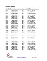
Page 25: ...ata 3 Int 12 Transmit Interrupt I O 13 Receive Data 3 Int 13 TX Frame Done I O 14 Transmit Clock 3 Int 14 Receive Interrupt I O 15 Receive Clock 3 Int 15 RX Abort Detected I O 16 Transmit Data 4 Int 16 Transmit Interrupt I O 17 Receive Data 4 Int 17 TX Frame Done I O 18 Transmit Clock 4 Int 18 Receive Interrupt I O 19 Receive Clock 4 Int 19 RX Abort Detected I O 20 Transmit Data 5 Int 20 Transmit ...

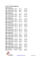
Page 26: ...lock I O 14 pin 15 pin 49 SDLC receive clock I O 15 pin 16 pin 50 SDLC channel 4 SDLC transmit data I O 16 pin 17 pin 51 SDLC receive data I O 17 pin 18 pin 52 SDLC transmit clock I O 18 pin 19 pin 53 SDLC receive clock I O 19 pin 20 pin 54 SDLC channel 5 SDLC transmit data I O 20 pin 21 pin 55 SDLC receive data I O 21 pin 22 pin 56 SDLC transmit clock I O 22 pin 23 pin 57 SDLC receive clock I O 2...

Page 27: ...id until that bit in the status register is explicitly cleared When an interrupt occurs the Master interrupt enable should be cleared and the status register read to determine the cause of the interrupt Next perform any processing needed to remove the interrupting condition clear the latched bit and set the Master interrupt enable bit high again The individual enables operate after the interrupt h...

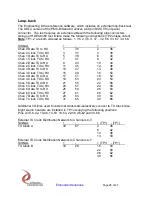
Page 28: ...han 2 Clock TX to RX 11 45 12 46 Chan 3 Data TX to RX 13 47 14 48 Chan 3 Clock TX to RX 15 49 16 50 Chan 4 Data TX to RX 17 51 18 52 Chan 4 Clock TX to RX 19 53 20 54 Chan 5 Data TX to RX 21 55 22 56 Chan 5 Clock TX to RX 23 57 24 58 Chan 6 Data TX to RX 25 59 26 60 Chan 6 Clock TX to RX 27 61 28 62 Chan 7 Data TX to RX 29 63 30 64 Chan 7 Clock TX to RX 31 65 32 66 Additional I O lines used for ex...

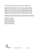
Page 29: ...19 to TP2 19 and TP1 53 to TP2 53 Channel 5 TP1 22 to 56 TP1 58 to 24 TP1 23 to TP2 23 and TP1 57 to TP2 57 Channel 6 TP1 26 to 60 TP1 62 to 28 TP1 27 to TP2 27 and TP1 61 to TP2 61 Channel 7 TP1 30 to 64 TP1 66 to 32 TP1 31 to TP2 31 and TP1 65 to TP2 65 Installing two shunts per channel on the headers in TP1 will connect the external clock to the respective channels removing them allows internal...

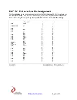
Page 30: ...cation and not needed by this design 12V unused 1 2 GND INTA 3 4 5 6 BUSMODE1 5V 7 8 9 10 GND 11 12 CLK GND 13 14 GND 15 16 5V 17 18 AD31 19 20 AD28 AD27 21 22 AD25 GND 23 24 GND C BE3 25 26 AD22 AD21 27 28 AD19 5V 29 30 AD17 31 32 FRAME GND 33 34 GND IRDY 35 36 DEVSEL 5V 37 38 GND LOCK 39 40 41 42 PAR GND 43 44 AD15 45 46 AD12 AD11 47 48 AD9 5V 49 50 GND C BE0 51 52 AD6 AD5 53 54 AD4 GND 55 56 AD...

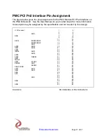
Page 31: ...igned by the specification and not needed by this design 12V unused 1 2 3 4 GND 5 6 GND 7 8 9 10 11 12 RST BUSMODE3 13 14 BUSMODE4 15 16 GND 17 18 AD30 AD29 19 20 GND AD26 21 22 AD24 23 24 IDSEL AD23 25 26 AD20 27 28 AD18 29 30 AD16 C BE2 31 32 GND 33 34 TRDY 35 36 GND STOP 37 38 PERR GND 39 40 SERR 41 42 C BE1 GND 43 44 AD14 AD13 45 46 GND AD10 47 48 AD8 49 50 AD7 51 52 53 54 GND 55 56 57 58 GND ...

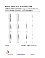
Page 32: ...O_5m 6 40 IO_6p IO_6m 7 41 IO_7p IO_7m 8 42 IO_8p IO_8m 9 43 IO_9p IO_9m 10 44 IO_10p IO_10m 11 45 IO_11p IO_11m 12 46 IO_12p IO_12m 13 47 IO_13p IO_13m 14 48 IO_14p IO_14m 15 49 IO_15p IO_15m 16 50 IO_16p IO_16m 17 51 IO_17p IO_17m 18 52 IO_18p IO_18m 19 53 IO_19p IO_19m 20 54 IO_20p IO_20m 21 55 IO_21p IO_21m 22 56 IO_22p IO_22m 23 57 IO_23p IO_23m 24 58 IO_24p IO_24m 25 59 IO_25p IO_25m 26 60 I...

Page 33: ...II when it is not powered can damage it as well as the rest of the host system This problem may be avoided by turning all power supplies on and off at the same time Alternatively the use of OPTO 22 isolation panels is recommended Keep cables short Flat cables even with alternate ground lines are not suitable for long distances The PMC BiSerial III does not contain special input protection The conn...

Page 34: ...nsertion easy and reliable The PMC is secured against the carrier with four screws attached to the 2 stand offs and 2 locations on the front panel The four screws provide significant protection against shock vibration and incomplete insertion The PMC Module provides a low temperature coefficient of 2 17 W oC for uniform heat This is based upon the temperature coefficient of the base FR4 material o...

Page 35: ...ompany the return Dynamic Engineering will not be responsible for damages due to improper packaging of returned items For service on Dynamic Engineering Products not purchased directly from Dynamic Engineering contact your reseller Products returned to Dynamic Engineering for repair by other than the original customer will be treated as out of warranty Out of Warranty Repairs Out of warranty repai...

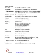
Page 36: ...ss Modes LW boundary Space see memory map Wait States 1 for all addresses Interrupt TX interrupt at end of message transmission TX interrupt at end of frame transmission RX interrupt at end of message reception RX interrupt when abort received Software interrupt I2O interrupts DMA No DMA Support implemented at this time Onboard Options All Options are Software Programmable Interface Options 68 pin...

Page 37: ...DLC Driver software and user application Data sheet reprints are available from the manufacturer s web site Note The Engineering Kit is strongly recommended for first time PMC BiSerial III purchases Schematics Schematics are provided as part of the engineering kit for customer reference only This information was current at the time the printed circuit board was last revised This revision letter is...

Reviews: