Embedded Solutions
Page 7 of 37
The PMC BiSerial-III conforms to the PMC and CMC draft standards. This guarantees
compatibility with multiple PMC Carrier boards. Because the PMC may be mounted on
different form factors, while maintaining plug and software compatibility, system
prototyping may be done on one PMC Carrier board, with final system implementation
uses a different one. Contact Dynamic Engineering for a copy of this specification. It is
assumed that the reader is at least casually familiar with this document and basic logic
design.
In standard configuration, the PMC BiSerial-III is a Type 1 mechanical with only low-
profile components on the back of the board and one slot wide, with 10 mm inter-board
height for the front panel, standoffs, and PMC connectors. The 10 mm height is the
"standard" height and will work in most systems with most carriers. If your carrier has
non-standard connectors (height) to mate with the PMC BiSerial-III, please let us know.
We may be able to do a special build with a different height connector to compensate.
The standard configuration shown in Figure 1 makes use of two external (to the Xilinx)
FIFOs. The FIFOs can be as large as 128K deep x 32 bits wide. Some designs do not
require so much memory, and are more efficiently implemented using the Xilinx internal
memory.
The SDLC implementation has sixteen 4 Kbyte Dual Port RAM (DPR) blocks
implemented using the Xilinx internal block RAM. Each channel has two associated
DPRs. Each DPR is configured to have a 32-bit port on the PCI side, and a 16-bit port
on the I/O side. See Figure 2 for a representation of the SDLC circuit.
The SDLC interface uses programmable PLL clock A as a reference frequency to
sample the internal or external transmitter clock. Clock and data in and out comprise
the four I/O lines of each SDLC channel. The two DPRs are partitioned into one block
each for transmit and receive. The RAM blocks are used as circular buffers that have
independently specified start and stop addresses and separate transmit and receive
interrupts.
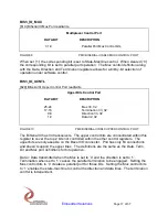
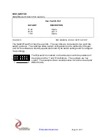
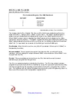
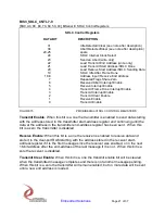
All the data I/O lines on the SDLC are programmable to be register controlled or state-
machine controlled. Any or all of the bits can be used as a parallel port instead of being
dedicated to a specific I/O protocol. Thirty-four differential I/O are provided at the front
bezel (32 of the 34 at Pn4) for the serial signals. The drivers and receivers conform to
the RS-485 specification (exceeds RS-422 specification). The RS-485 input signals are
selectively terminated with 100Ω. The termination resistors are in two-element
packages to allow flexible termination options for custom formats and protocols.
Optional pull-up/pull-
down resistor packs can also be installed to provide a logic ‘1’
when the lines are not driven. The terminations and transceivers are programmable
through the Xilinx device to provide the proper mix of outputs and inputs and
terminations needed for a specific protocol implementation. The terminations are
programmable for all I/O.


