EM78P911A
8-bit Micro-controller
__________________________________________________________________________________________________________________________________________________________________
* This specification is subject to change without notice.
~ ~
39
12/19/2005 (V2.1)
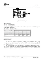
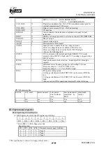
ERS=0 => CA-1=0 HIGH ORDER DATA
CA-1=1 LOW ORDER DATA
CA0~CA14
O
Program code address bus. CA0~CA14 are address output pins for
external programming ROM access.
CD0~CD12
I
Data access in terms of CA0 ~ CA12 addressing.
IOD0~IOD7
O
I/O data bus.
INSEND
O
Used to indicate the instruction completion and ready for next
instruction.
IRSEL
O
IRSEL is an output pin used to select an external EVEN/ODD ROM.
PH1OUT
O
Phase 1 output
X2OUT O System
clock
output.
/HOLD I Microcontroller
hold
request.
/POVD
I
Input pin used to enable Power on voltage detector.
Power on voltage detector is enabled if /POVD is low.
Power on voltage detector is disabled if /POVD is high.
Also see the following table.
ENTCC I TCC control pin with internal pull-high (560K
Ω
). TCC works
normally when ENTCC is high, and TCC counting is stopped when
ENTCC is low.
MCLK
I
Input pin for main clock selection. Internal pull low through a
register.
CWFS
I
Minimum access frequency range for call waiting CAS tone.
Frequency range is +/-0.5% if CWFS is low.
Frequency range is +/- 1.5% if CWFS is high.
R32k
I
R5 register setting option
4-bit page selection and 4-bit PORT5 I/O can be access if R32k is
low.
5-bit page selection and 5-bit PORT5 I/O can be access if R32k is
high
Also see section III for operational register R5 in the following.
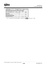
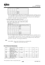
POVD status table
/POVD
2.2V reset
power on reset
Low power
detect without
reset
Low power detect
controlled by
RA(5)
sleep mode
current
1 No yes Yes
Yes
1uA
0 Yes yes Yes
yes
15uA
III. Operational registers
R5 (Program Page Select Register)
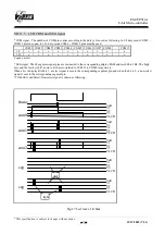
(1) If R32k pin is low level, the R5 register is as follows.
7 6 5 4 3 2 1 0
R57 R56 R55 R54 PS3 PS2 PS1 PS0
* Bit 0 (PS0) ~ 3 (PS3) Page select bits
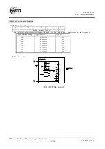
Page select bits
PS3 PS2 PS1
PS0 Program
memory page (Address)
0 0 0 0 Page
0
0 0 0 1 Page
1
0 0 1 0 Page
2

