
Registers
STA309A
28/67
Doc ID 13855 Rev 4
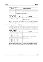
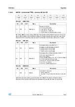
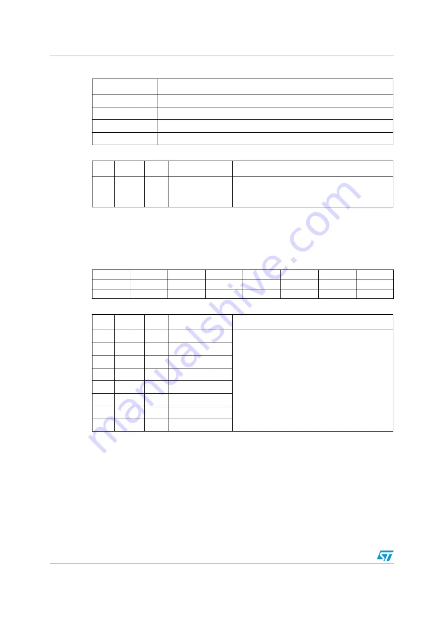
Setting the MPC bit turns on special processing that corrects the STA50x power device at
high power. This mode should lower the THD+N of a full STA50x DDX system at maximum
power output and slightly below. This mode will only be operational in OM[1,0] = 01.
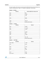
7.2.5 Configuration
register E (0x04)
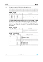
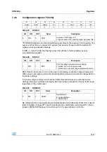
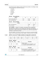
Each individual channel output can be set to output a binary PWM stream. In this mode
output A of a channel will be considered the positive output and output B is negative inverse.
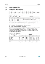
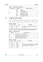
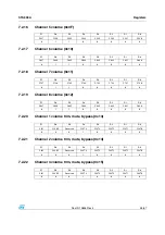
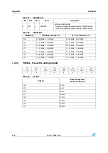
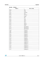
Table 24.
CSZ definition
CSZ[4:0]
Compensating pulse size
00000
0 clock period compensating pulse size
00001
1 clock period compensating pulse size
…
…
11111
31 clock period compensating pulse size
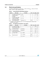
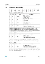
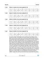
Table 25.
MPC bit
Bit
RW
RST
Name
Description
7
RW
1
MPC
Max power correction:
1: enable STA50x correction for THD reduction near
maximum power output.
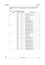
D7
D6
D5
D4
D3
D2
D1
D0
C8BO
C7BO
C6BO
C5BO
C4BO
C3BO
C2BO
C1BO
0
0
0
0
0
0
0
0
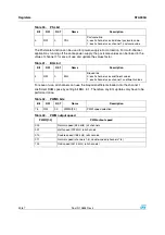
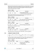
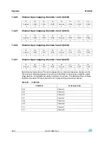
Table 26.
CnBO bits
Bit
RW
RST
Name
Description
0
RW
0
C1BO
Channels 1, 2, 3, 4, 5, 6, 7, and 8 binary output
mode enable bits:
0: ordinary DDX tristate output
1: binary output mode.
1
RW
0
C2BO
2
RW
0
C3BO
3
RW
0
C4BO
4
RW
0
C5BO
5
RW
0
C6BO
6
RW
0
C7BO
7
RW
0
C8BO


