Virtex-6 FPGA System Monitor
31
UG370 (v1.1) June 14, 2010
System Monitor Calibration
are monitored via the JTAG TAP during device power down. During power down the
System Monitor uses an internal oscillator instead of DCLK. On power up several DCLK
cycles will be required to resynchronize the DRP ( see
System Monitor Timing, page 33
A second user-programmable temperature threshold level (Control register
50h
) is used to
carry out a user-defined thermal management procedure, such as powering-on or
controlling the speed of a fan. An alarm signal (ALM[0]) becomes active when the FPGA
temperature exceeds the limit in this register. The signal is available through the
interconnect and is routed using the FPGA resources. The alarm signal resets when the
temperature falls below the threshold in Control register
54h
. This operation
differs
for the
supply-sensor alarm, because the supply alarm resets when the measurement is between
the upper and lower thresholds.
Thermal Diode (DXP and DXN)
Previous generations of Virtex FPGAs allowed users to monitor the die temperature by
providing access to a PN junction (diode) on the die. By connecting this diode to an
external signal conditioning IC (thermal monitor), the die temperature could be
determined. To preserve backward compatibility with these thermal monitoring solutions
and to facilitate production test requirements, the thermal diode is also available on
Virtex-6 FPGAs. The thermal diode can be accessed by using the DXP and DXN pins in
bank 0. The thermal diode is independent of System Monitor, and its use in no way affects
the System Monitor operation. If the thermal diode is not being used, these pins should be
tied to ground. The thermal diode has a non-ideality factor of ~1.0002 and a series
resistance of < 2
Ω
. For implementation details, consult the data sheet for the selected
external thermal monitoring IC.
System Monitor Calibration
The Virtex-6 FPGA System Monitor can digitally calibrate out any offset-and-gain errors in
the ADC and supply sensor (see
for an explanation of offset and
gain errors). By connecting known voltages (V
REFN
and V
REFP
) to the ADC and supply
sensor, the offset-and-gain errors can be calculated and correction coefficients generated.
System Monitor has a built-in calibration function that calculates these coefficients
automatically. By initiating a conversion on ADC channel 8 (
08h
), all calibration
coefficients are calculated and then applied during normal operation when calibration is
enabled. BUSY transitions High for the duration of the entire calibration sequence. This
calibration sequence is three times longer than a regular conversion on a sensor channel.
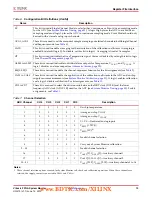
These calibration coefficients are applied to measurements by setting the calibration enable
bits in Configuration Register 1. See
Note:
Calibration must be enabled to meet the specified performance of the ADC and sensors.
Even if the ADC is only being used to monitor external analog inputs, calibration should be enabled.
www.BDTIC.com/XILINX

