SERIES AP220 / AP231 ACROPACK
USER
’S MANUAL
Acromag, Inc. Tel: 248-295-0310
- 18 -
http://www.acromag.com
- 18 -
https://www.acromag.com
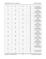
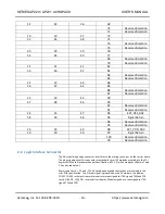
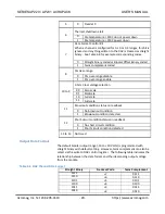
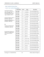
Table 3.3 Location Register
Note that any registers/bits not
mentioned will remain at the
default value logic low.
This feature was implemented
on the Revision B boards.
Bit(s)
FUNCTION
2 to 0
Module Site Location Bits. These bits identify the location on
the carrier of the AP module.
000
Carrier Site A
001
Carrier Site B
010
Carrier Site C
011
Carrier Site D
7 to 3
Module Slot Location Bits. These bits identify the slot location
of the AP module in a system. The Carrier may use backplane
signals as in a VPX system or a carrier DIP switch to uniquely
identify the system location of the carrier.
XXXXX
System Slot identification bits are described by the
AcroPack carrier card.
31 to 8 Not Used
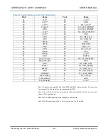
DAC Channel Registers (Read/Write) - (BAR0 + 0x0000 0008 to 0x0000 0044)
Sixteen (16) DAC Channels registers are used to write and read the DAC 24-bit
control/data values. Writing to the address of the specific register enables
transfer of data and control of the DAC. Read of the specified register returns
the DAC data or control value as requested. All reads requires write of two
read commands to complete serial shift out of the DAC data or control value.
Then read the DAC channel register will contain the read data in the lower 16
bits for AP231 and bits-15 to 4 of the AP220. See Table 3.5 for the allowed
DAC write and read commands.
The contents of the DAC Channel registers are transferred to their
corresponding converter input buffer serially. This serial data transfer take
1.6µs. Thus, a new write of the same DAC register can be performed no
sooner then 1.6µs after the previous write. A DAC Write Status register, at
base address plus 54H, is available as a write operation busy status indicator.
The channels Status bit will be set low upon initiation of a write operation
and will remain low until the requested write operation has completed. New
write accesses to the same DAC Channel register, should not be initiated
unless its write busy status bit is set high. Read of the DAC registers must
also wait 1.6µs after issue of two read commands. Thus you avoid read of the
register as it is being serially shift out.
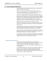
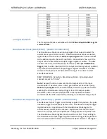
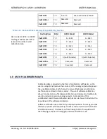
Table 3.4 DAC Channel Register
Bit(s)
FUNCTION
15 to 0
Data 16-bits or Control register data with issue of 0100
commend or DAC data when issued of 0001 or 0011.
19 to 16
Address 4-bits
0000 No Operation
0001
Write to input register
(no DAC output update input
register only written.) Used for simultaneous mode


