Series AVME9125 VMEbus 6U Analog Input Board
___________________________________________________________________________________________
- 10 -
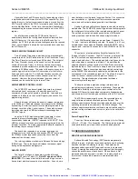
At least 5
µ
seconds of input acquire time should be provided
after programming of the Control register and Start Value register
before a Software Start Convert command is issued. These
configuration registers control the on board multiplexers which
select a channel for input to the converter.
Offset Coefficient Register (Read/Write, 54H)
This Offset Coefficient register is read/writeable and is used to
store the offset coefficient to 1/4 bit resolution. The least
significant 10 bits of the register comprise the offset coefficient
stored as a two’s complement value. Bits 15 to 10 of the register
are not used. The weight corresponding to bits 9 to 0 are shown in
the last row of the table below.
Offset Coefficient Register
7 Bits and a Sign Bit
2 Bits to 1/4
Bit
Resolution
D9
D8
D7
D6
D5
D4
D3
D2
D1
D0
Sign
2
6
2
5
2
4
2
3
2
2
2
1
2
0
2
-1
2
-2
-128
64
32
16
8
4
2
1
1/2
1/4
In an ideal system, the offset coefficient would be exactly 0.
The deviation from 0 provides correction for the actual circuit
components. The offset coefficient should be determined by
taking several readings (e.g. 64) of the auto zero calibration
voltage and then averaging the several auto zero values measured
to provide the offset coefficient. Several auto zero values
averaged together reduce the measurement uncertainty.
Refer to the “Programming Considerations for Acquiring
Analog Inputs” section for details on how to acquire auto zero
values for determination of the offset coefficient.
An example illustrating how the offset coefficient value is
determined for the offset of -9.25 is presented here. Since the
offset value desired (-9.25) is negative, the sign bit D9 must be
set. If the offset were a positive value then the sign bit D9 would
not be set.
We continue by working in order from bit D8 down to bit D0.
The current offset (-128) with bit D9 only set is less than -9.25 thus
bit D8 must also be set. The offset with bits D9 and D8 set is now
-64 (-128+64). A bit can be set if the offset value resulting is less
then or equal to the target offset value. Since -64 is < -9.25, we
must also set bits D7, and D6. The offset with bits D9, D8, D7,
and D6 set correspond to an offset of -16 (-128+64+32+16). We
now continue to bit D5 and determine we can not set this bit since
this would give and offset of -8 which is greater then -9.5. Bits D4
and D3 must be set to give an offset of -10. Bit D2 can not be set
since an offset of -9 would result and -9 is greater then -9.25.
Finally bits D1 and D0 are also set. The value written to the offset
coefficient must be 3DB hex as seen in the table below.
3
D
B
1
1
1
1
0
1
1
0
1
1
D9
D8
D7
D6
D5
D4
D3
D2
D1
D0
-128
64
32
16
8
4
2
1
1/2
1/4
The Offset Coefficient register can be read or written via 16-bit
or 8-bit data transfers. In addition, the register contents are
cleared upon reset.
Gain Coefficient Registers (Read/Write, 56H & 58H)
The Gain Coefficient registers are read/writeable and are used
to store the gain coefficient to 1/4 bit resolution. A gain coefficient
is a 19-bit value; thus, two 16-bit registers are used to hold a gain
coefficient. The least significant 16 bits are stored in one register
while the most significant 3 bits are stored in the other.
Registers at addresses 56H and 58H are used to hold the
most significant and least significant parts of the gain coefficient
corresponding to channels 0 to 31.
The least significant 16 bits and most significant 3 bits of the
gain coefficient are shown in the following table. The weight
corresponding to each bit is also given in the table. Refer to the
“Programming Considerations for Acquiring Analog Inputs” section
for details on how to determine the gain coefficient.
The Gain Coefficient value is determined by working in order
from bit D2 of the most significant gain register down to bit D0 of
the least significant gain register. A bit can be set if the gain value
resulting is less then or equal to the target gain value.
Most Significant Gain Coefficient Register
Data Bits 15 to 8 of Most Significant Word
Not Used
Data Bits 7 to 0 of Most Significant Word
D07
D06
D05
D04
D03
D02
D01
D00
Not Used
2
0
2
-1
2
-2
Least Significant Gain Coefficient Register
Data bits 15 to 8 of Least Significant Word
D15
D14
D13
D12
D11
D10
D09
D08
2
-3
2
-4
2
-5
2
-6
2
-7
2
-8
2
-9
2
-10
Data bits 7 to 0 of Least Significant Word
D07
D06
D05
D04
D03
D02
D01
D00
2
-11
2
-12
2
-13
2
-14
2
-15
2
-16
2
-17
2
-18
In an ideal system, the gain coefficient would be exactly 1.
The deviation from 1 provides correction for the actual circuit
components. A gain coefficient of 1 is obtained by writing a value
of 4 hex to the Most Significant Gain Coefficient register and a
value of 0 to the Least Significant Gain Coefficient register.
The Gain Coefficient register can be read or written via 16-bit
or 8-bit data transfers. Upon reset the register contents will be set
to a gain coefficient of 0 which will result in a digital values of zero
in the mailbox registers.
Artisan Technology Group - Quality Instrumentation ... Guaranteed | (888) 88-SOURCE | www.artisantg.com


