Series AVME9125 VMEbus 6U Analog Input Board
___________________________________________________________________________________________
- 6 -
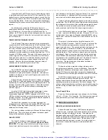
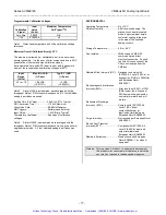
DATA TRANSFER TIMING
VMEbus data transfer time is measured from the falling edge
of DSx* to the falling edge of DTACK* during a normal data
transfer cycle. Typical transfer times are given in the following
table.
Register
Data Transfer Time
All Registers
800 nS, Typical.
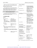
FIELD GROUNDING CONSIDERATIONS
The AVME9125 board is designed with passive filters on each
supply line. This provides maximum filtering and signal isolation
between the AVME9125 board and the VMEbus system.
However, the boards are considered non-isolated, since there is
electrical continuity to the VMEbus grounds. Care should be taken
in designing installations without isolation to avoid ground loops
and noise pickup. This is particularly important for analog I/O
applications when a high level of accuracy/resolution is needed.
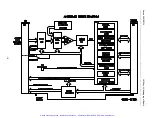
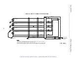
A signal being measured cannot be floating—it must be
referenced to analog common on the AVME9125. See Drawing
4501-688 for analog input connections for differential inputs.
3.0 PROGRAMMING INFORMATION
This Section provides the specific information necessary to
operate the AVME9125 non-intelligent VMEbus board.
The board is addressable on 256 byte boundaries in the Short
I/O (A16) Address Space. This Acromag VMEbus non-intelligent
slave has a Board Status register and Card Identification
information. The 256 bytes of memory consumed by the board is
composed of Card Identification, Status, Control, and Converted
Data registers. The memory map for AVME9125 is shown in
Tables 3.1 and 3.2.
MEMORY MAP
Table 3.1: AVME9125 6U Bd Short I/O Memory Map
Base
Addr+
EVEN Byte
D15 D08
ODD Byte
D07 D00
Base
Addr+
00
↓
3E
Card Identification
Space
Not Used
Card Identification
Space
Low Byte
01
↓
3F
40
Status Register
41
42
Control Register
43
44
Timer Prescaler
Interrupt Vector
Register
45
46
Conversion Timer
47
48
End Channel
Value
Start Channel
Value
49
4A
New Data Register
Channels 0 to 15
4B
4C
New Data Register
Channels 16 to 31
4D
4E
Missed Data Register
Channels 0 to 15
4F
50
Missed Data Register
Channels 16 to 31
51
Base
Addr+
EVEN Byte
D15 D08
ODD Byte
D07 D00
Base
Addr+
52
Not Used
Bits15 to Bit 01
Start Convert
Bit-0
53
54
Offset Coefficient
55
56
MSW of Gain Coefficient
57
58
LSW of Gain Coefficient
59
5A
Not Used
1
5B
5C
Not Used
1
5D
5E
Not Used
1
5F
60
Mail Box Ch 00
61
62
Mail Box Ch 01
63
64
Mail Box Ch 02
65
66
Mail Box Ch 03
67
68
Mail Box Ch 04
69
6A
Mail Box Ch 05
6B
6C
Mail Box Ch 06
6D
6E
Mail Box Ch 07
6F
70
Mail Box Ch 08
71
72
Mail Box Ch 09
73
74
Mail Box Ch 10
75
76
Mail Box Ch 11
77
78
Mail Box Ch 12
79
7A
Mail Box Ch 13
7B
7C
Mail Box Ch 14
7D
7E
Mail Box Ch 15
7F
80
Mail Box Ch 16
81
82
Mail Box Ch 17
83
84
Mail Box Ch 18
85
86
Mail Box Ch 19
87
88
Mail Box Ch 20
89
8A
Mail Box Ch 21
8B
8C
Mail Box Ch 22
8D
8E
Mail Box Ch 23
8F
90
Mail Box Ch 24
91
92
Mail Box Ch 25
93
94
Mail Box Ch 26
95
96
Mail Box Ch 27
97
98
Mail Box Ch 28
99
9A
Mail Box Ch 29
9B
9C
Mail Box Ch 30
9D
9E
Mail Box Ch 31
9F
A0
Not Used
1
A1
↓
↓
↓
FE
Not Used
1
FF
Notes (Table 3.1):
1. The board will not respond to addresses that are "Not Used".
This memory map reflects byte accesses using the “Big
Endian” byte ordering format. Big Endian is the convention used
in the Motorola 68000 microprocessor family and is the VMEbus
convention. In Big Endian, the lower-order byte is stored at odd-
byte addresses. The Intel x86 family of microprocessors uses the
opposite convention, or “Little Endian” byte ordering. Little Endian
uses even-byte addresses to store the low-order byte.
Artisan Technology Group - Quality Instrumentation ... Guaranteed | (888) 88-SOURCE | www.artisantg.com


