Series AVME9125 VMEbus 6U Analog Input Board
___________________________________________________________________________________________
- 15 -
Upon initiation of an A/D convert cycle, the analog input data
is digitized and stored into an internal A/D Converter buffer. Also
during this cycle, the last converted data value is moved from the
A/D Converter buffer to the FPGA for correction and then storage
into the Mail Box Buffer. At this time, the New Data Available bit
corresponding the previous converted channel is set in the FPGA
register.
For all other scan modes the FPGA control logic will
automatically discard the first digitized data value received from
the A/D Converter. It is not written to the Mail Box buffer. In
addition, the FPGA logic also automatically generates the required
“flush” convert signals to obtain the last converted data value from
the A/D Converter.
TIMED PERIODIC TRIGGER CIRCUIT
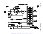
Timed Periodic Triggering is provided by two programmable
counters (an 8-bit Timer Prescaler and a 16-bit Conversion Timer).
The Timer Prescaler is clocked by an 8MHz clock. The output of
the Timer Prescaler counter is then used to clock the second
counter (Conversion Timer). In this way, the two counters are
cascaded to provide variable time periods anywhere from 11.25
µ
seconds to 2.0889 seconds. The output of the second counter is
used to trigger the start of new A/D conversions for the Uniform
Scan modes of operation. For the Burst Continuous mode, the
interval between conversions of each channel is fixed at
≅
15
µ
seconds. However, the interval between the group (burst) of
channels can be controlled by the Interval Timer.
VME INTERRUPT CONTROL LOGIC
The AVME9125 can be configured to generate an interrupt
after completion of conversion of a single channel or after
conversion of a group of channels is completed. Interrupts are
enabled on the board via the Control Register (see section 3 for
programming details).
A board interrupt will cause the board to release the interrupt
to the VMEbus. The board releases the interrupt to the VMEbus
by asserting the interrupt request level as pre-programmed in the
Interrupt Level bits of the Control register. The board’s interrupt
logic then monitors the VMEbus Interrupt Acknowledge Input
(IACKIN*) signal.
An active IACKIN* signal, detected by the board, is either
passed to Interrupt Acknowledge Output (IACKOUT*) or
consumed by the board. IACKIN* is passed to IACKOUT* if the
VMEbus interrupt level does not match that programmed into the
Interrupt Level bits. If a match is detected, the board responds to
the interrupt by consuming IACKIN*.
The board also responds to an interrupt by placing the
interrupt vector on the data bus and asserts DTACK* active, and
the VMEbus master responds by executing the code at the
address of the interrupt vector.
The interrupt release mechanism is Release On Acknowledge
(ROAK) type. That is, the board will release the request signal
during an interrupt acknowledge cycle.
ANALOG INPUTS
The field I/O interface to the board is provided through
connector P2 (refer to Table 2.3).
Field I/O signals are NON-
ISOLATED.
This means that the field return and logic common
have a direct electrical connection to each other. As such, care
must be taken to avoid ground loops (see Section 2 for connection
recommendations). Ignoring this effect may cause operation
errors, and with extreme abuse, possible circuit damage.
Analog inputs and calibration voltages are selected via analog
multiplexers. The AVME9125 control logic automatically programs
the multiplexers for selection of the required analog input channel.
The multiplexer control is based upon selection of differential
analog input and the Start and End channel register values.
Up to 32 differential inputs can be monitored. Channel’s 0 to
15 + and - inputs are individually selected. Channels 16 to 31 are
multiplexed on the companion Expander board (EXP9125) and a
and - input pair is connected to the AVME9125 via the P2
connector.
The output of a Instrumentation Amplifier feeds the A/D
(Analog to Digital) Converter. The A/D Converter is a state of the
art, 16-bit, successive approximation converter with a built-in
sample and hold circuit. The sample and hold circuit goes into the
hold mode when a conversion is initiated. This maintains the
selected channel’s voltage constant until the A/D has accurately
digitized the input. Then it returns to sample mode to acquire the
next channel. Once a conversion has been started, control logic
on the AVME9125 automatically updates the multiplexers for the
next channel to be converted as required. This allows the input to
settle for the next channel while the previous channel is
converting. This pipelined mode of operation facilitates a
maximum system throughput.
The board contains a precision voltage reference and a
ground (autozero) reference for use in calibration. These provide
considerable flexibility in obtaining accurate calibration for the
desired A/D Converter range when compared to fixed hardware
potentiometers for offset and gain calibration of the A/D Converter.
The FPGA will automatically correct the converted data by
using software calculated offset and gain coefficients. The
software calculated coefficients should be updated whenever the
operating temperature environment of the board changes. The
software calculated calibration coefficients are calculated using the
precision voltage reference and auto zero (refer to the calibration
section).
Power Supply Filters
Power line filters are dedicated to each supply line for filtering
of the +5, +15, and -15 volt supplies. The filters provide improved
noise performance as is required on precision analog boards.
5.0 SERVICE AND REPAIR
SERVICE AND REPAIR ASSISTANCE
Surface-Mounted Technology (SMT) boards are generally
difficult to repair. It is highly recommended that a non-functioning
board be returned to Acromag for repair. The board can be
damaged unless special SMT repair and service tools are used.
Further, Acromag has automated test equipment that thoroughly
checks the performance of each board. When a board is first
produced and when any repair is made, it is tested, placed in a
burn-in room at elevated temperature, and retested before
shipment.
Artisan Technology Group - Quality Instrumentation ... Guaranteed | (888) 88-SOURCE | www.artisantg.com

