Series AVME9125 VMEbus 6U Analog Input Board
___________________________________________________________________________________________
- 12 -
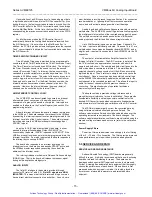
Interrupts can be enabled to activate after conversion of each
channel or the group of channels as defined by the Start and End
Channel Values. If interrupts are configured to go active after the
conversion of each channel, the actual interrupt will be issued
every 15
µ
seconds. If interrupt upon completion of a group of
channels is selected, an interrupt will be issued
≅
25.5
µ
seconds
after conversion of the last channel in the group has started.
At this time 15
µ
seconds between interrupts is not sufficient
time to perform back to back interrupt acknowledge cycles on the
VME and PC platforms. Thus, interrupting after each channel is
converted cannot be recommended.
Burst Single-Mode
In burst single mode of operation conversions are performed
once for all channels (in sequential order) starting with Start
Channel and ending with the End Channel. The interval between
conversions of each channel is fixed at
≅
15
µ
seconds. The
interval timer has no functionality in this mode of operation.
After software selection of the burst single mode of operation,
conversions are started either by an external trigger, or by setting
the software start convert bit.
Interrupts can be enabled to activate after conversion of each
channel or the group of channels as defined by the Start and End
Channel Values. If interrupts are configured to go active after the
conversion of each channel, an interrupt will be issued every 15
µ
seconds (not recommended). If interrupt upon completion of a
group of channels is selected, an interrupt will be issued 25.5
µ
seconds after conversion of the last channel has started.
PROGRAMMING CONSIDERATIONS FOR ACQUIRING
ANALOG INPUTS
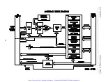
The AVME9125 board register architecture makes the
configuration fast and easy. The only set of configuration
hardware jumpers is for the base address of the board in the
VMEbus short I/O space. Once the board is mapped to the
desired base address, communication with the board registers is
straightforward.
USE OF CALIBRATION SIGNALS
Reference signals for analog input calibration have been
provided to improve the accuracy over the uncalibrated state. The
use of calibration allows the elimination of hardware calibration
potentiometers traditionally used in precision analog front ends.
The AVME9125 provides DSP (Digital Signal Processing)
logic for real-time calibration of digitized values. The on-board
hardware implements the required multiplication to adjust the gain
and also the summation to correct the offset. The gain and offset
coefficients required to implement this calibration must be
determined by software and stored in AVME9125 register before
conversion are triggered to obtain calibrated digital values (refer to
the memory map for these register locations). The reset condition
of the offset and gain coefficients are zero which will result in
digital values of zero in the mailbox registers.
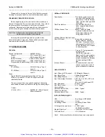
Uncalibrated Performance
The uncalibrated performance is affected by two primary error
sources. These are the Instrumentation Amplifier and the Analog
to Digital Converter (ADC). The instrumentation amplifier and
ADC have significant offset and gain errors (see specifications in
chapter 6) which reveal the need for software calibration.
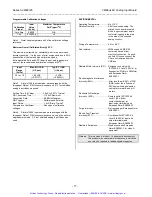
Calibrated Performance
Very accurate gain and offset coefficients for the AVME9125
can be calculated by using the calibration voltages present on the
board. The voltage reference and the analog ground (auto zero
signal) are used to determine two points of a straight line which
defines the analog input characteristic. The calibration reference
voltage is precisely adjusted at the factory to provide optimum
performance, as detailed in chapter 6.
Equation (1) following is used to correct the actual ADC data
(i.e. the uncorrected bit count read from the ADC) making use of
the calibration voltages.
[
] [
]
CorrectedCount = CountActual
OffsetCoef * GainCoef (1)
−
[
]
CorrectedCount = CountActual
Count
0V
*
32,080
Count
9.79V
Count
0V
(2)
−
−
By comparison of equations (1) and (2) it can be seen that the
offset coefficient = Count0V and the gain coefficient is the term
given in equation (3):
GainCoef =
Count
9.79V
Count
0V
(3)
32 080
,
−
Where:
Count9.79V
=
Actual ADC Data Read With
9.790039V Calibration Voltage
Applied
Count0V
=
Actual ADC Data Read With
Auto Zero Calibration Voltage
Applied
CountActual
=
Actual Uncorrected ADC Data
For Input Being Measured
The calibration gain and offset coefficients should not be
determined immediately after startup but after the module has
reached a stable temperature and updated periodically (e.g. once
an hour, or more often if ambient temperatures change) to obtain
the best accuracy. Note that several readings (e.g. 64) of the
calibration parameters should be taken via the ADC and averaged
to reduce the measurement uncertainty, since these points are
critical to the overall system accuracy.
Artisan Technology Group - Quality Instrumentation ... Guaranteed | (888) 88-SOURCE | www.artisantg.com


