background image

Series AVME9125                                                                                                     VMEbus 6U Analog Input Board
___________________________________________________________________________________________

- 8 -

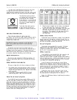
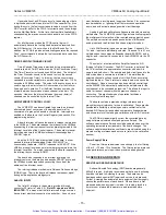
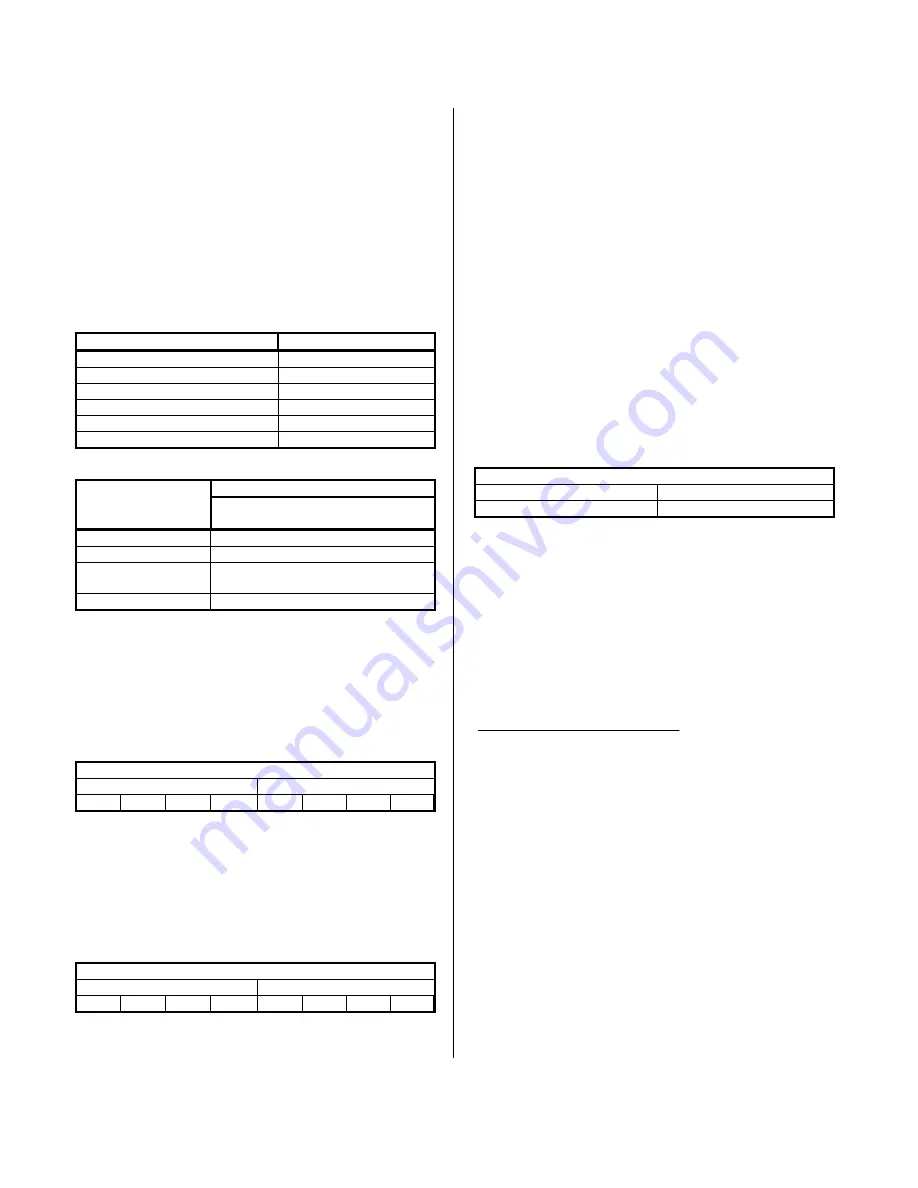
The function of each of the control register bits are described

in Table 3.3.  The control register can be read or written with either
8-bit or 16-bit data transfers.  A power-up or system reset sets all
control register bits to zero.

Analog Input Range and Corresponding Digital Output Code

The ideal input voltage corresponding to the 

±

10 volt input

range is given in Table 3.4.  In Table 3.5 the digital output code
corresponding to each of the ideal analog input values is given.
The hex codes for the converted digital output values are returned
in binary two’s complement format.

Table 3.4: Supported Full-Scale Ranges and Ideal Analog
Input

DESCRIPTION

ANALOG INPUT

Input Range

±

10V

LSB (Least Significant Bit) Weight

305

µ

V

+ Full Scale Minus One LSB

9.999695Volts

Midscale

0V

One LSB Below Midscale

-305

µ

V

 - Full Scale

-10V

Table 3.5:  Digital Output Codes and Input Voltages

DIGITAL OUTPUT

Binary 2’s Comp

DESCRIPTION

(Hex Code)

+ Full Scale - 1 LSB

7FFF

Midscale

0000

1 LSB Below
Midscale

FFFF

 - Full Scale

8000

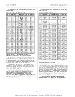
Interrupt Vector Register (Read/Write, 45H)

The Vector Register can be written with an 8-bit interrupt

vector.  This vector is provided to the system bus upon an active
interrupt acknowledge cycle.  Read or writing to this register is
possible via 16-bit or 8-bit data transfers.  16-bit data transfers will
implement simultaneous access of the Interrupt Vector and Timer
Prescaler registers.  The register contents are cleared upon reset.

Interrupt Vector Register

MSB

LSB

07

06

05

04

03

02

01

00

Interrupts are released on an interrupt acknowledge cycle.

Reading of the interrupt vector during an interrupt acknowledge
cycle signals the board to remove its interrupt request.

Timer Prescaler Register (Read/Write, 44H)

The Timer Prescaler register can be written with an 8-bit value

to control the time interval between conversions.

Timer Prescaler Register

MSB

LSB

15

14

13

12

11

10

09

08

This 8-bit number divides an 8 MHz clock signal.  The clock

signal is further divided by the number held in the Conversion

Timer Register.  The resulting frequency can be used to generate
periodic triggers for precisely timed intervals between conversions.

The Timer Prescaler has a minimum allowed value

restriction of 5A hex or 90 decimal.

  A Timer Prescaler value of

less then 90 (decimal) will result in an empty Mail Box Register
buffer.

Read or writing to this register is possible via 16-bit or 8-bit

data transfers.  A 16-bit data transfer will implement simultaneous
access to the Interrupt Vector and Timer Prescaler registers.  The
Timer Prescaler register contents are cleared upon reset.

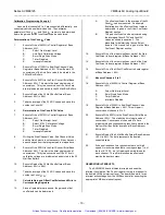
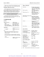
The formula used to calculate and determine the desired

Timer Prescaler value is given in the Conversion Timer section
which follows immediately.

Conversion Timer Register (Read/Write, 46H)

The Conversion Timer Register can be written to control the

interval time between conversions.  Read or writing this register is
possible with either 16-bit or 8-bit data transfers.  This register’s
contents are cleared upon reset.

Conversion Timer Register

MSB

LSB

15   14   13  12  11  10  09  08

07  06  05  04  03  02  01  00

This 16-bit number is the second divisor of an 8MHz clock

signal and is used together with the Timer Prescaler Register to
derive the frequency of periodic triggers for precisely timed
intervals between conversions.

The interval time between conversions is generated by

cascading two counters.  The first counter, the Timer Prescaler, is
clocked by an 8MHz clock signal.  The output of this clock is input
to the second counter, the Conversion Timer, and this output is
used to generate periodic trigger pulses.  The time period between
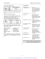
trigger pulses is described by the following equation:

Timer Prescaler   Conversion Timer = T in   seconds

8

µ

Where:

T

 = time period between trigger pulses in microseconds.

Timer Prescaler

 can be any value between 90 and 255 

decimal.

Conversion Timer

 can be any value between 1 and 

65,535 decimal.

The maximum period of time which can be programmed to

occur between conversions is (255 

 65,535) 

÷

 8 = 2.0889

seconds.  The minimum time interval that can be programmed to
occur is 11.25

µ

 seconds which can be implemented as (90 

 1) 

÷

8.  Any combination of the Timer Prescaler and Conversion Timer
are allowed as long as the Timer Prescaler value used is not
programmed to a value below 90 decimal.

Artisan Technology Group - Quality Instrumentation ... Guaranteed | (888) 88-SOURCE | www.artisantg.com

Summary of Contents for AVME9125 Series

Page 1: ...ess underutilized and idle equipment along with credit for buybacks and trade ins Custom engineering so your equipment works exactly as you specify Critical and expedited services Leasing Rentals Demo...

Page 2: ...South Wixom Road P O BOX 437 Wixom MI 48393 7037 U S A Tel 248 624 1541 Fax 248 624 9234 Copyright 1998 Acromag Inc Printed in the USA Data and specifications are subject to change without notice 8500...

Page 3: ...CONTROL LOGIC 15 ANALOG INPUTS 15 Power Supply Filters 15 5 0 SERVICE AND REPAIR 15 SERVICE AND REPAIR ASSISTANCE 15 PRELIMINARY SERVICE PROCEDURE 16 6 0 SPECIFICATIONS 16 PHSICAL 16 VMEbus COMPLIANC...

Page 4: ...or upon completion of conversion of the group of all scanned channels Software Programmable Interrupt Level The VMEbus interrupt level is software programmable Additional registers are associated wit...

Page 5: ...rs for different base address locations is shown in Table 2 1 IN means that the pins are shorted together with a shorting clip OUT indicates that the clip has been removed The jumper locations are sho...

Page 6: ...ME9125 The EXP9125 will pull CHSel0 high when present Lastly the AVME9125 provides 15 volts to the EXP9125 via the P2 connector Pin assignments for the P2 connectors of the AVME9125 are shown in Table...

Page 7: ...Identification Space Not Used Card Identification Space Low Byte 01 3F 40 Status Register 41 42 Control Register 43 44 Timer Prescaler Interrupt Vector Register 45 46 Conversion Timer 47 48 End Channe...

Page 8: ...is set to 0 Reset condition Set to 0 Bit 0 EXP9125 Board Present Status Read This bit will be 1 when the EXP9125 Expander board is present in a slot adjacent to the AVME9125 A set bit indicates that 3...

Page 9: ...gister The resulting frequency can be used to generate periodic triggers for precisely timed intervals between conversions The Timer Prescaler has a minimum allowed value restriction of 5A hex or 90 d...

Page 10: ...tiated with the Software Start Convert command This is done to avoid mistaking data from an old scan cycle with that of a new scan cycle The New Data registers can be read via 16 bit or 8 bit data tra...

Page 11: ...e an offset of 10 Bit D2 can not be set since an offset of 9 would result and 9 is greater then 9 25 Finally bits D1 and D0 are also set The value written to the offset coefficient must be 3DB hex as...

Page 12: ...econds after the programmed interval has lapsed If interrupt upon completion of a group of channels is selected an interrupt will be issued 10 5 seconds after the interval time of the last selected ch...

Page 13: ...tal Signal Processing logic for real time calibration of digitized values The on board hardware implements the required multiplication to adjust the gain and also the summation to correct the offset T...

Page 14: ...Corresponding Registers 13 Since all parameters are known the gain and offset coefficients can be determined A The offset coefficient is the average of the 32 Count0V values measured An example illus...

Page 15: ...cally 800ns for accesses to the AVME9125 board registers The board s FPGA monitors the base address jumper setting which is jumperable on 256 byte boundaries in the VMEbus Short I O A16 Address Space...

Page 16: ...o Table 2 3 Field I O signals are NON ISOLATED This means that the field return and logic common have a direct electrical connection to each other As such care must be taken to avoid ground loops see...

Page 17: ...al 600mA Maximum VMEbus COMPLIANCE Specification This device meets or exceeds all written VME specifications per revision C 1 dated October 1985 IEC 821 1987 and IEEE 1014 1987 Data Transfer Bus A16 D...

Page 18: ...the uniform single sample mode A 3 foot shielded analog input ribbon was used ENVIRONMENTAL Operating Temperature 0 to 70 C Relative Humidity 5 95 non condensing The printed circuit board is coated w...

Page 19: ...VMEbus 6U Analog Input Board ___________________________________________________________________________________________ 18 Artisan Technology Group Quality Instrumentation Guaranteed 888 88 SOURCE ww...

Page 20: ...VMEbus 6U Analog Input Board ___________________________________________________________________________________________ 19 Artisan Technology Group Quality Instrumentation Guaranteed 888 88 SOURCE ww...

Page 21: ...SHIELDED CABLE IS RECOMMENDED FOR LOWEST NOISE SHIELD IS CONNECTED TO GROUND REFERENCE AT ONE END ONLY TO PROVIDE SHIELDING WITHOUT GROUND LOOPS NOTES CH16 31 EXT SOURCE 16 31 SEE NOTE 2 SEE NOTE 1 SH...

Page 22: ...uipment Have surplus equipment taking up shelf space We ll give it a new home Learn more Visit us at artisantg com for more info on price quotes drivers technical specifications manuals and documentat...

Reviews: