Achieving good signal integrity becomes difficult in this scenario because the
TMS
and
TCK
signals are
branched at T-junctions. The signal integrity of the
TMS
signal is not important because until a rising
edge of
TCK
signal is detected, it is ignored by the target device. The signal integrity of the
TCK
signal
is important because any false edges cause the target device to sample
TDI
and
TMS
signals too many
times. Sampling the
TDI
and
TMS
signals too many times corrupts the serial data stream that is seen by
the target devices.
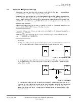
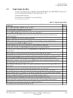
To avoid this issue, always use buffering where the
TCK
signal is split:
Debug
Connector
TDI
TMS
TCK
TDO
Target
Device
TDI
TMS
TCK
TDO
Target
Device
TDI
TMS
TCK
TDO
Figure 3-8 Daisy-chained JTAG connection with TCK buffers
The solution in the above figure prevents the two
TCK
branches from interacting and ensures good
signal integrity with minimal overshoot. You must place buffers and series termination resistors as close
as possible to the T-junction of the
TCK
signal.
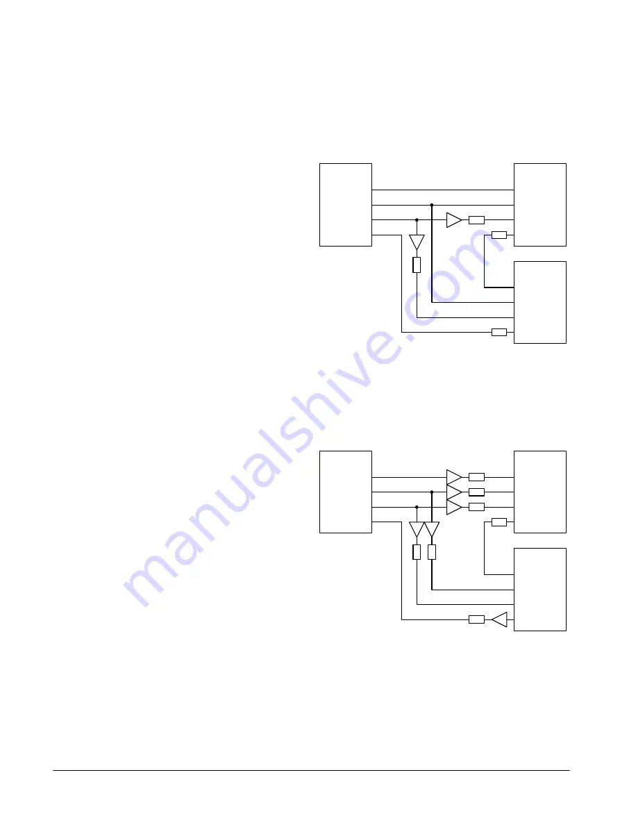
This causes some skew between the
TDI
,
TMS
, and
TCK
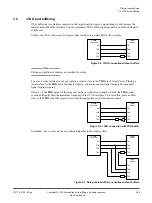
signals. To correct this skew, use the same
type of buffers on the
TDI
,
TMS
, and
TCK
signals. For example:
Debug
Connector
TDI
TMS
TCK
TDO
Target
Device
TDI
TMS
TCK
TDO
Target
Device
TDI
TMS
TCK
TDO
Figure 3-9 Fully buffered JTAG connection
3 Target board design
3.2 JTAG port buffering
101714_0100_02_en
Copyright © 2019 Arm Limited or its affiliates. All rights reserved.
3-56
Non-Confidential

