AD9776A/AD9778A/AD9779A
Rev. B | Page 31 of 56
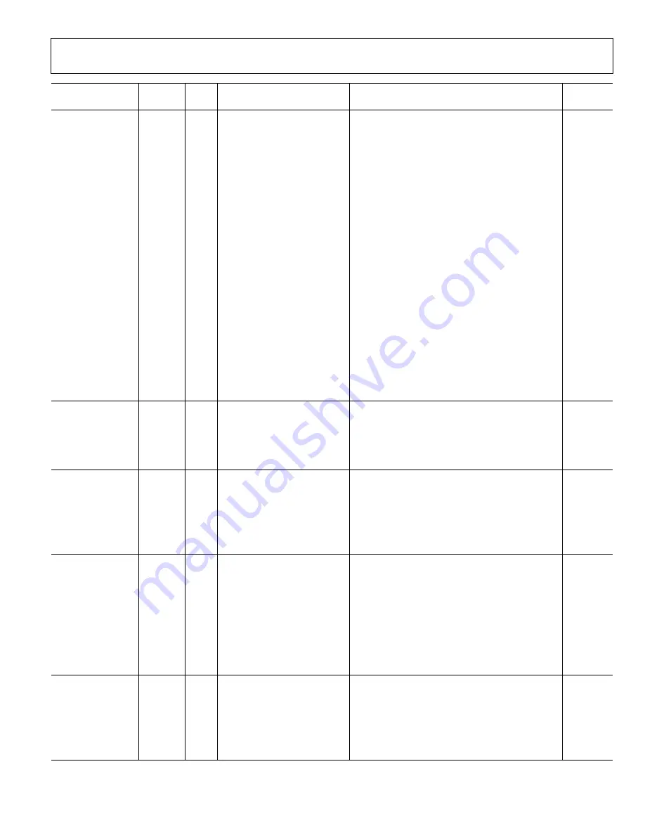
Register
Address
Bits
Register Name
Parameter
Function
Default
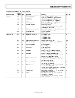
PLL Control
0x08
7:2
PLL Band Select[5:0]
This sets the operating frequency range of the
VCO. For details (see Table 23).
111001
0x08 1:0
PLL
VCO
Drive[1:0]
Controls the signal strength of the VCO output. Set
to 11 for optimal performance.
11
0x09 7 PLL
enable
0: PLL off, DAC sample clock is sourced directly by
the REFCLK input.
1: PLL on, DAC clock synthesized internally from
REFCLK input via PLL clock multiplier.
0
0x09 6:5
PLL
VCO
Divide
Ratio[1:0] Sets the value of the VCO output divider, which
determines the ratio of the VCO output frequency
to the DAC sample clock frequency, f
VCO
/f
DACCLK
.
00: f
VCO
/f
DACCLK
= 1.
01: f
VCO
/f
DACCLK
= 2.
10: f
VCO
/f
DACCLK
= 4.
11: f
VCO
/f
DACCLK
= 8.
10
0x09
4:3
PLL Loop Divide Ratio[1:0]
Sets the value of the DACCLK divider, which
determines the ratio of the DAC sample clock
frequency to the REFCLK frequency, f
DACCLK
/f
REFCLK
.
00: f
DACCLK
/f
REFCLK
= 2.
01: f
DACCLK
/f
REFCLK
= 4.
10: f
DACCLK
/f
REFCLK
= 8.
11: f
DACCLK
/f
REFCLK
= 16.
10
0x09 2:0
PLL
Bias[2:0]
Controls VCO bias current. Set to 011 for optimal
performance.
010
Misc. Control
0x0A
7:5
VCO Control Voltage[2:0]
(read only)
000 to 111, proportional to voltage at VCO control
voltage input, readback only. A value of 011
indicates the VCO centered in its frequency range.
000
0x0A
4:0
PLL Loop Bandwidth[4:0]
Controls the bandwidth of the PLL filter. Increasing
the value lowers the loop bandwidth. Set to 01111
for optimal performance.
11111
I DAC Control
0x0C
0x0B
1:0
7:0
I DAC Gain Adjustment[9:8]
I DAC Gain Adjustment[7:0]
The I DAC Gain Adjustment[9:0] value is the I DAC
10-bit gain setting word. Bit 9 is the MSB and Bit 0
is the LSB.
01
11111001
0x0C
7
I DAC sleep
0: I DAC on.
1: I DAC off, but reference remains powered.
0
0x0C
6
I DAC power-down
0: I DAC on.
1: I DAC off.
0
Aux DAC1 Control
0x0E
0x0D
1:0
7:0
Auxiliary DAC1 Data[9:8]
Auxiliary DAC1 Data[7:0]
The auxiliary DAC 1 Data [9:0] value is the Aux DAC1
10-bit output current control word. Magnitude of
the auxiliary DAC current increases with increasing
value. Bit 9 is the MSB and Bit 0 is the LSB.
00
00000000
0x0E
7
Auxiliary DAC1 sign
0: AUX1_P active.
1: AUX1_N active.
0
0x0E 6 Auxiliary DAC1 current
direction
0: source.
1: sink.
0
0x0E
5
Auxiliary DAC1 power-down
0: auxiliary DAC1 on.
1: auxiliary DAC1 off.
0
Q DAC Control
0x10
0x0F
1:0
7:0
Q DAC Gain Adjustment[9:8]
Q DAC Gain Adjustment[7:0]
The Q DAC Gain Adjustment[9:0] value is the Q DAC
10-bit gain setting word. Bit 9 is the MSB and Bit 0
is the LSB.
01
11111001
0x10
7
Q DAC sleep
0: Q DAC on.
1: Q DAC off.
0
0x10
6
Q DAC power-down
0: Q DAC on.
1: Q DAC off.
0

