ADM1060
Rev. B | Page 34 of 52
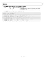
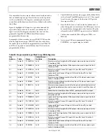
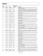
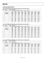
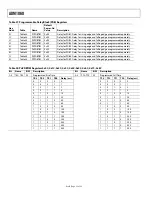
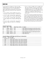
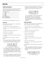
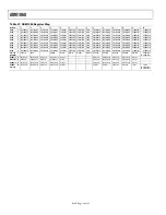
Table 39. Programmable Driver Outputs Registers
Hex
Address Table
Name
Default
Power-On
Value Description
P1PDOCFG
0x00 Selects the format of the PDO1 output (open drain, open drain with internal
pull-up, charge pumped, etc.).
P2PDOCFG
0x00 Selects the format of the PDO2 output (open drain, open drain with internal
pull-up, charge pumped, etc.).
P3PDOCFG
0x00 Selects the format of the PDO3 output (open drain, open drain with internal
pull-up, charge pumped, etc.).
P4PDOCFG
0x00 Selects the format of the PDO4 output (open drain, open drain with internal
pull-up, charge pumped, etc.).
P5PDOCFG
0x00 Selects the format of the PDO5 output (open drain, open drain with internal
pull-up, etc.). Note: charge pumped output is not available on this driver.
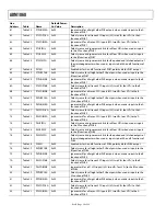
P6PDOCFG
0x00 Selects the format of the PDO6 output (open drain, open drain with internal
pull-up, etc.). Note: charge pumped output is not available on this driver.
P7PDOCFG
0x00 Selects the format of the PDO7 output (open drain, open drain with internal
pull-up, etc.). Note: charge pumped output is not available on this driver.
P8PDOCFG
0x00 Selects the format of the PDO8 output (open drain, open drain with internal
pull-up etc.). Note: charge pumped output is not available on this driver.
P9PDOCFG
0x00 Selects the format of the PDO9 output (open drain, open drain with internal
pull-up, etc.). Note: charge pumped output is not available on this driver.
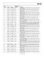
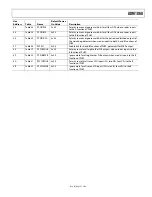
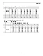
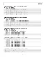
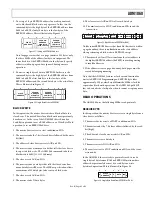
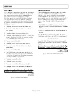
Table 40. PnPDOCFG Register 0x0D, 0x1D, 0x2D, 0x3D, 0x4D, 0x5D, 0x6D, 0x7D, 0x8D (Power-On Default 0x00)
Bit Name
R/W
Description
7
Reserved
N/A
Cannot Be Used
Controls the logical state of the PDO. These three bits determine what effect, if any, the logi-
cal input to the PDO has on its output.
CFG6 CFG5 CFG4 PDO
State
0
0
0
0
Disabled, with weak pull-down
0 0 1 PLB_OUT
Enabled,
follows PLB logic output
0
1
0
0
Enables SMBus data, drive low
0
1
1
1
Enables SMBus data, drive high
6–4 CFG6–CFG4
R/W
1
X
X
MCLK
Enables MCLK out onto pin
CFG3
CFG2
CFG1
CFG0
Pull-Up Supply
Pull-Up Strength
0 0 0 X none
N/A
0
0
1
X
VCP
300 kΩ
0 1 0 0 VP1
Low
0 1 0 1 VP1
High
0 1 1 0 VP2
Low
0 1 1 1 VP2
High
1 0 0 0 VP3
Low
1 0 0 1 VP3
High
1 0 1 0 VP4
Low
1 0 1 1 VP4
High
1 1 1 0 V
DD
Low
3–0 CFG3–CFG0
R/W
1 1 1 1 V
DD
High

