ADM1060
Rev. B | Page 43 of 52
SCL
SDA
START BY MASTER
1
9
1
9
A1
A0
R/W
1
D7
D6
D5
D4
D3
D2
D1
D0
0
0
1
1
ACK. BY
SLAVE
FRAME 1
SLAVE ADDRESS
FRAME 2
COMMAND CODE
ACK. BY
SLAVE
SCL
(CONTINUED)
D7
D6
D5
D4
D3
D2
D1
D0
ACK. BY
SLAVE
1
9
1
9
D7
D6
D5
D4
D3
D2
D1
D0
ACK. BY
SLAVE
STOP
BY
MASTER
FRAME N
DATA BYTE
FRAME 3
DATA BYTE
SDA
(CONTINUED)
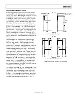
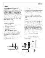
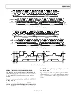
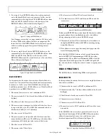
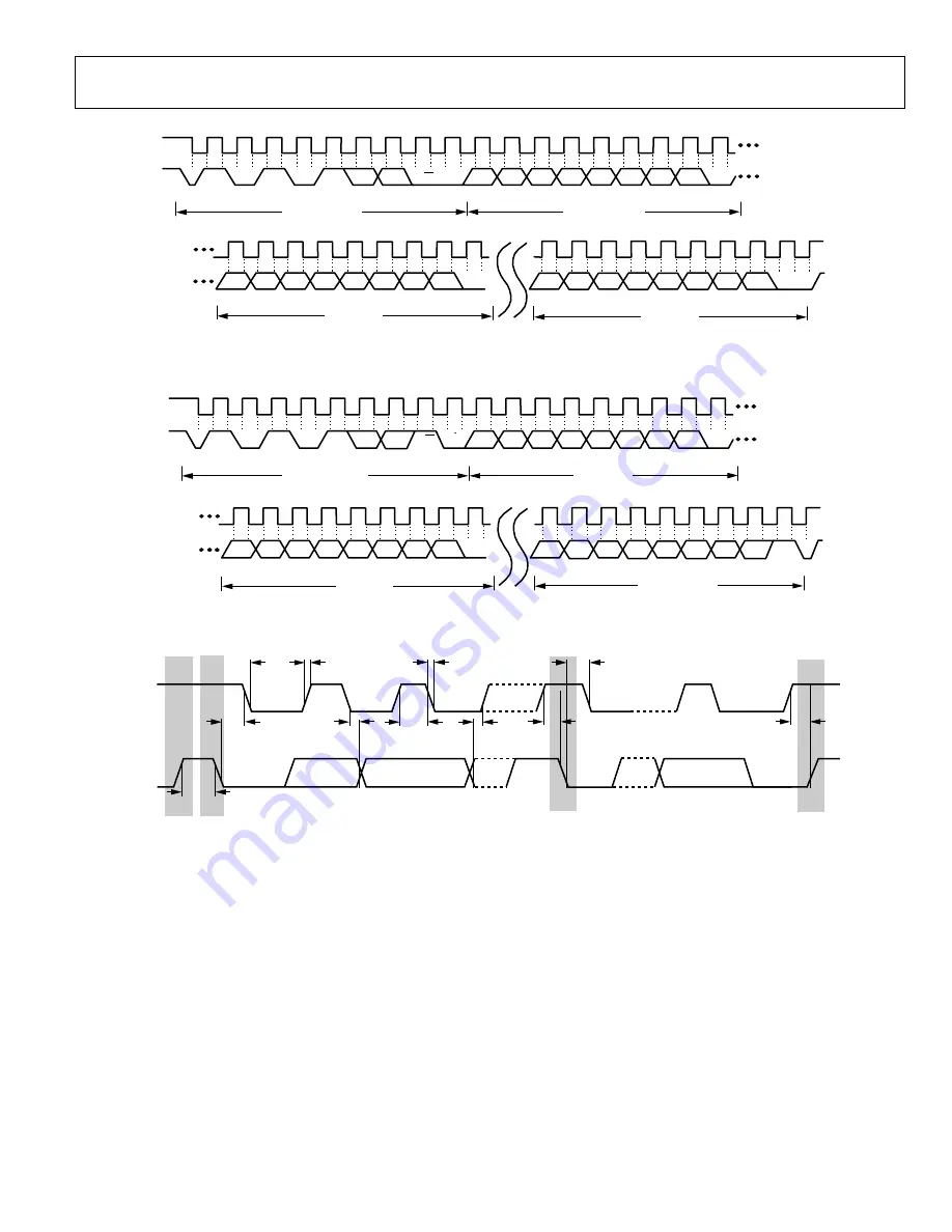
Figure 25. General SMBus Write Timing Diagram
SCL
SDA
START BY MASTER
SCL
(CONTINUED)
SDA
(CONTINUED)
A1
A0
R/W
1
0
0
1
1
D7
D6
D5
D4
D3
D2
D1
D0
ACK. BY
MASTER
FRAME 1
SLAVE ADDRESS
FRAME 2
DATA BYTE
1
9
1
9
ACK. BY
SLAVE
1
9
D7
D6
D5
D4
D3
D2
D1
D0
D7
D6
D5
D4
D3
D2
D1
D0
NO ACK.
ACK. BY
MASTER
1
9
STOP
BY
MASTER
FRAME 3
DATA BYTE
FRAME N
DATA BYTE
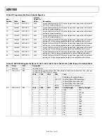
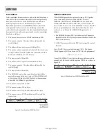
Figure 26. General SMBus Read Timing Diagram
SCL
SCL
SDA
P
S
t
HD;STA
t
HD;DAT
t
HIGH
t
SU;DAT
t
SU;STA
t
HD;STA
t
F
t
R
t
LOW
t
BUF
t
SU;STO
P
S
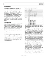
Figure 27. Serial Bus Timing Diagram
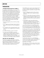
SMBus PROTOCOLS FOR RAM AND EEPROM
The ADM1060 contains volatile registers (RAM) and nonvola-
tile EEPROM. User RAM occupies address locations from 0x00
to 0xDF, while EEPROM occupies addresses from 0xF800 to
0xF9FF.
Data can be written to and read from both RAM and EEPROM
as single data bytes.
Data can be written only to unprogrammed EEPROM locations.
To write new data to a programmed location, it is first necessary
to erase it. EEPROM erasure cannot be done at the byte level;
the EEPROM is arranged as 16 pages of 32 bytes, and an entire
page must be erased.
Page erasure is enabled by setting Bit 3 in register UPDCFG
(address 0x90) to 1. If this is not set, page erasure cannot occur,
even if the command byte (0xFE) is programmed across the
SMBus.

