Rev. 2.10
238
���� 02� 201�
Rev. 2.10
239
���� 02� 201�
HT68F20/HT68F30/HT68F40/HT68F50/HT68F60
HT68FU30/HT68FU40/HT68FU50/HT68FU60
Enhanced I/O Flash Type 8-Bit MCU with EEPROM
HT68F20/HT68F30/HT68F40/HT68F50/HT68F60
HT68FU30/HT68FU40/HT68FU50/HT68FU60
Enhanced I/O Flash Type 8-Bit MCU with EEPROM
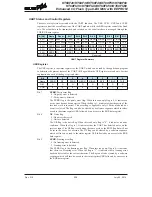
• UART receiver
The UART is capable of receiving word lengths of either 8 or 9 bits can be selected by
programming the BNO bit in the UCR1 register. When BNO bit is set, the word length will be
set to 9 bits. In this case the 9th bit, which is the MSB, will be stored in the RX8 bit in the UCR1
register. At the receiver core lies the Receiver Shift Register more commonly known as the RSR.
The data which is received on the RX external input pin is sent to the data recovery block. The
data recovery block operating speed is 16 times that of the baud rate, while the main receive
serial shifter operates at the baud rate. After the RX pin is sampled for the stop bit, the received
data in RSR is transferred to the receive data register, if the register is empty. The data which
is received on the external RX input pin is sampled three times by a majority detect circuit to
determine the logic level that has been placed onto the RX pin. It should be noted that the RSR
register, unlike many other registers, is not directly mapped into the Data Memory area and as
such is not available to the application program for direct read/write operations.
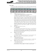
• Receiving data
When the UART receiver is receiving data, the data is serially shifted in on the external RX input
pin to the shift register, with the least significant bit LSB first. The RXR register is a four byte
deep FIFO data buffer, where four bytes can be held in the FIFO while the 5th byte can continue
to be received. Note that the application program must ensure that the data is read from RXR
before the 5th byte has been completely shifted in, otherwise the 5th byte will be discarded and
an overrun error OERR will be subsequently indicated. The steps to initiate a data transfer can be
summarized as follows:
♦
Make the correct selection of the BNO, PRT, PREN and STOPS bits to define the required
word length, parity type and number of stop bits.
♦
Setup the BRG register to select the desired baud rate.
♦
Set the RXEN bit to ensure that the UART receiver is enabled and the RX pin is used as a
UART receiver pin.
At this point the receiver will be enabled which will begin to look for a start bit.
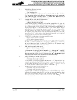
When a character is received, the following sequence of events will occur:
♦
The RXIF bit in the USR register will be set then RXR register has data available, at least three
more character can be read.
♦
When the contents of the shift register have been transferred to the RXR register and if the RIE
bit is set, then an interrupt will be generated.
♦
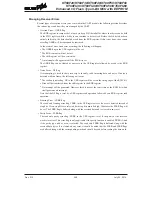
If during reception, a frame error, noise error, parity error or an overrun error has been detected,
then the error flags can be set.
The RXIF bit can be cleared using the following software sequence:
1. A USR register access
2. A RXR register read execution

