7.4.6 Device Reset and Fault Management
This section provides the details of power-on-reset (POR), software reset, and other diagnostics and fault-
management features of DACx300x.
7.4.6.1 Power-On Reset (POR)
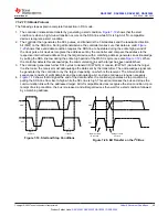
The DACx300x family of devices includes a power-on reset (POR) function that controls the output voltage at
power up. After the V
DD
supply has been established, a POR event is issued. The POR causes all registers
to initialize to default values, and communication with the device is valid only after a POR (boot-up) delay. The
default value for all the registers in the DACx300x is loaded from NVM as soon as the POR event is issued.
When the device powers up, a POR circuit sets the device to the default mode.
indicates that the
POR circuit requires specific V
DD
levels to make sure that the internal capacitors discharge and reset the device
at power up. To make sure that a POR occurs, V
DD
must be less than 0.7 V for at least 1 ms. When V
DD
drops
to less than 1.65 V, but remains greater than 0.7 V (shown as the undefined region), the device may or may
not reset under all specified temperature and power-supply conditions. In this case, initiate a POR. When V
DD
remains greater than 1.65 V, a POR does not occur.
No power-on reset
Power-on reset
0.7 V
Undefined
0 V
1.65 V
1.71 V
5.5 V
V
DD
(V)
Spe cified supply
voltage range
Figure 7-13. Threshold Levels for V
DD
POR Circuit
7.4.6.2 External Reset
An external reset to the device can be triggered through the GPIO pin or through the register map. To initiate a
device software reset event, write reserved code 1010 to the RESET field in the COMMON-TRIGGER register.
A software reset initiates a POR event.
shows how the GPIO pin can be configured as a RESET pin.
This configuration must be programmed into the NVM so that the setting is not cleared after the device reset.
The RESET input must be a low pulse. The device starts the boot-up sequence after the falling edge of the
RESET input. The rising edge of the RESET input does not have any effect.
7.4.6.3 Register-Map Lock
The DACx300x implement a register-map lock feature that prevents an accidental or unintended write to the
DAC registers. The device locks all the registers when the DEV-LOCK bit in the COMMON-CONFIG register
is set to 1. However, the software reset function through the COMMON-TRIGGER register is not blocked
when using the I
2
C interface. To bypass the DEV-LOCK setting, write 0101 to the DEV-UNLOCK bits in the
COMMON-TRIGGER register.
DAC53001, DAC53002, DAC63001, DAC63002
SLASF48 – MAY 2022
Copyright © 2022 Texas Instruments Incorporated
43
Product Folder Links:


