7.5.2 I
2
C Programming Mode
The DACx300x devices have a 2-wire serial interface (SCL and SDA), and one address pin (A0); see also
2
C bus consists of a data line (SDA) and a clock line (SCL) with pullup structures. When the bus is idle,
both SDA and SCL lines are pulled high. All the I
2
C-compatible devices connect to the I
2
C bus through the open
drain I/O pins, SDA and SCL.
The I
2
C specification states that the device that controls communication is called a
controller
, and the devices
that are controlled by the controller are called
targets
. The controller generates the SCL signal. The controller
also generates special timing conditions (start condition, repeated start condition, and stop condition) on the bus
to indicate the start or stop of a data transfer. Device addressing is completed by the controller. The controller
on an I
2
C bus is typically a microcontroller or digital signal processor (DSP). The DACx300x family operates as
a target on the I
2
C bus. A target acknowledges controller commands, and upon controller control, receives or
transmits data.
Typically, the DACx300x family operates as a target receiver. A controller writes to the DACx300x, a target
receiver. However, if a controller requires the DACx300x internal register data, the DACx300x operate as a
target transmitter. In this case, the controller reads from the DACx300x. According to I
2
C terminology, read and
write refer to the controller.
The DACx300x family supports the following data transfer modes:
• Standard mode (100 kbps)
• Fast mode (400 kbps)
• Fast mode plus (1.0 Mbps)
The data transfer protocol for standard and fast modes is exactly the same; therefore, both modes are referred
to as
F/S-mode
in this document. The fast mode plus protocol is supported in terms of data transfer speed,
but not output current. The low-level output current would be 3 mA; similar to the case of standard and fast
modes. The DACx300x family supports 7-bit addressing. The 10-bit addressing mode is not supported. The
device supports the general call reset function. Sending the following sequence initiates a software reset within
the device: start or repeated start, 0x00, 0x06, stop. The reset is asserted within the device on the rising edge of
the ACK bit, following the second byte.
Other than specific timing signals, the I
2
C interface works with serial bytes. At the end of each byte, a ninth clock
cycle generates and detects an acknowledge signal. An acknowledge is when the SDA line is pulled low during
the high period of the ninth clock cycle.
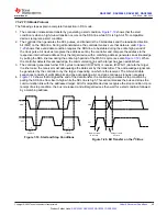
depicts a not-acknowledge, when the SDA line is left high
during the high period of the ninth clock cycle.
Data output
by transmitter
Data output
by receiver
SCL from
controller
1
2
S
Start
condition
8
9
Not acknowledge
Acknowledge
Clock pulse for
acknowledgement
Figure 7-18. Acknowledge and Not Acknowledge on the I
2
C Bus
DAC53001, DAC53002, DAC63001, DAC63002
SLASF48 – MAY 2022
48
Copyright © 2022 Texas Instruments Incorporated
Product Folder Links:


