7.4.7 Power-Down Mode
The DACx300x output amplifier and internal reference can be independently powered down through the EN-
INT-REF, VOUT-PDN-X, and IOUT-PDN-X bits in the COMMON-CONFIG register (see also
). At
power up, the DAC output and the internal reference are disabled by default. In power-down mode, the DAC
outputs (OUTx pins) are in a high-impedance state. To change this state to 10 kΩ
‑
A
GND
or 100 kΩ
‑
A
GND
in
voltage-output mode (at power up), use the VOUT-PDN-X bits. The power-down state for current-output mode is
always high-impedance.
The DAC power-up state can be programmed to any state (power-down or normal mode) using the NVM.
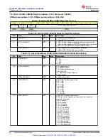
shows the DAC power-down bits. The individual channel power-down bits can be mapped to the GPIO
pin using the GPIO-CONFIG register. This function is called sleep mode. In this mode, the internal low-dropout
regulator (LDO) and the common functional blocks are still powered-on, and the device draws a maximum of
28 μA of current through the power supply.
Table 7-11. DAC Power-Down Bits
REGISTER
VOUT-PDN-X[1]
VOUT-PDN-X[0]
IOUT-PDN-X
DESCRIPTION
COMMON-CONFIG
0
0
1
Power up VOUT-X
0
1
1
Power down VOUT-X with 10 kΩ to AGND.
Power down IOUT-X to Hi-Z.
1
0
1
Power down VOUT-X with 100 kΩ to AGND.
Power down IOUT-X to Hi-Z.
1
1
1
Power down VOUT-X to Hi-Z.
Power down IOUT-X to Hi-Z (default).
1
1
0
Power down VOUT-X to Hi-Z.
Power up IOUT-X.
7.4.7.1 Deep-Sleep Mode
The DACx300x provide a deep-sleep mode, where the internal LDO and most of the common functional blocks
are powered-down. The GPIO pin must be used to enter and exit this mode. The I
2
C or SPI interface does not
work during the deep-sleep mode. The steps to enter and exit the deep-sleep mode are:
1. Make sure that the GPIO pin is pulled high.
2. Write 1 to the DEEP-SLEEP-EN bit in the GPIO-CONFIG register.
3. Disable GP output and SDO by writing 0 to GPO-EN and SDO-EN bits.
4. Enable GPIO input mode by writing 1 to GPI-EN and 0b0000 to GPI-CONFIG bits.
5. To program these settings into the NVM, write 1 to the NVM-PROG bit in the COMMON-TRIGGER register.
6. A negative-edge trigger on the GPIO puts the device into the deep-sleep mode. The LDO takes
approximately 550 μs to switch off. The device remains in this mode as long as the signal is low.
7. To bring the device out of the deep-sleep mode, pull the GPIO pin high. The digital circuitry and the LDO
take approximately 550 μs to switch on.
DAC53001, DAC53002, DAC63001, DAC63002
SLASF48 – MAY 2022
Copyright © 2022 Texas Instruments Incorporated
45
Product Folder Links:


