AD9779
Preliminary Technical Data
Rev. PrD | Page 16 of 34
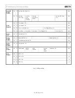
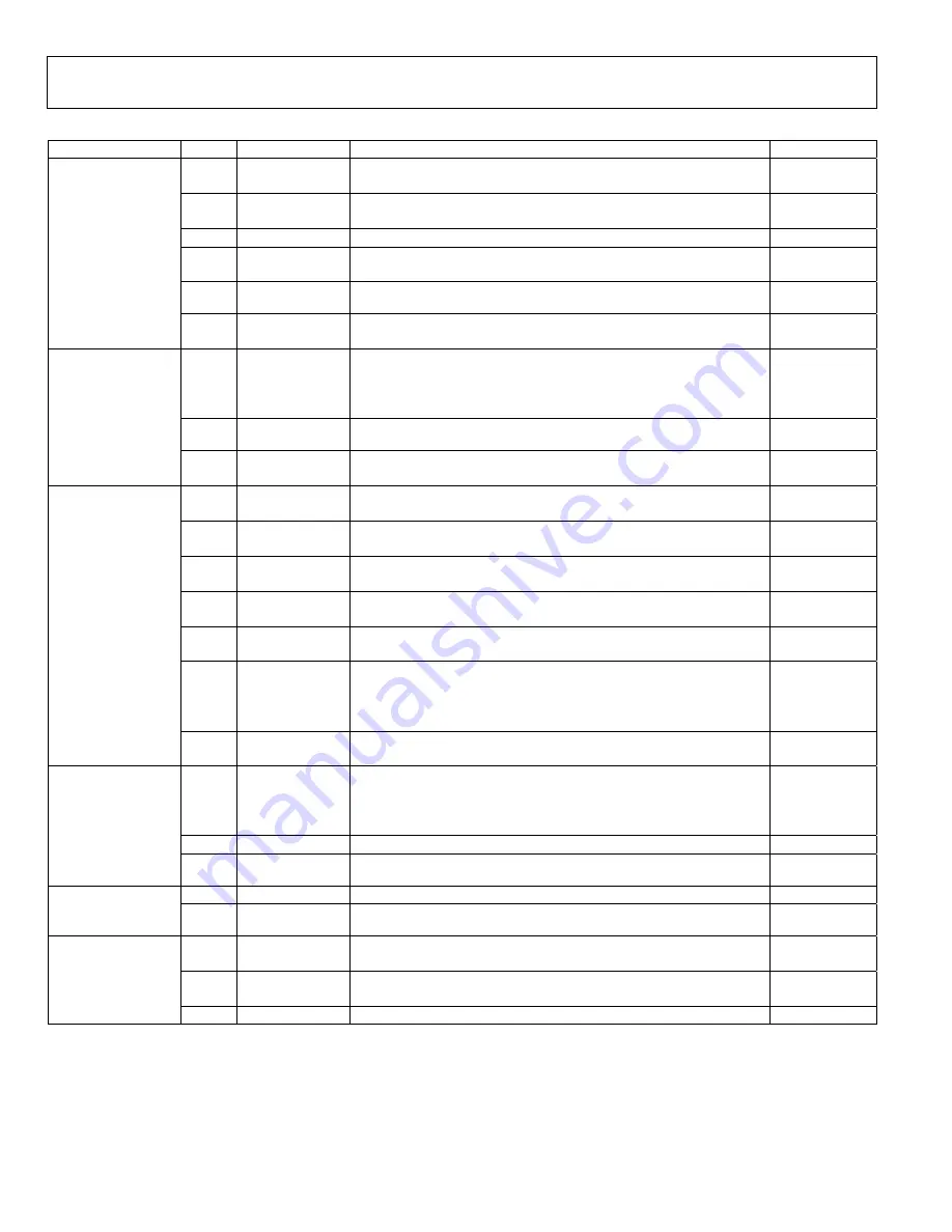
Register (hex)
Bits
Name Function
Default
7
SDIO Bidirectional
0: Use SDIO pin as input data only
1: Use SDIO as both input and output data
0
6
LSB/MSB First
0: First bit of serial data is MSB of data byte
1: First bit of serial data is LSB of data byte
0
5
Software RESET
Bit must be written with a 1, then 0 to soft reset SPI register map
0
4 Power
Down
Mode
0: All circuitry is active
1: Disable all digital and analog circuitry, only SPI port is active
0
3
Auto Power Down
Enable
0
00
Comm Register
1
PLL LOCK (read
only)
0: PLL is not locked
1: PLL is locked
0
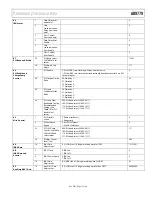
7:6 Filter
Interpolation
Rate
00: 1x interpolation
01: 2x interpolation
10: 4x interpolation
11: 8x interpolation
00
5:2 Control
Halfband
Filters 1,2,3
See
Table 13
for filter modes
0000
01
Digital Path Filter
Control
0
Zero Stuffing
0: Zero stuffing off
1: Zero stuffing on
0
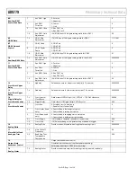
7
Data Format
0: Signed binary
1: Unsigned binary
0
6
One Port Mode
0: Both input data ports receive data
1: Data port 1 only receives data
0
5
Real Mode
0: Enable Q path for signal processing
1: Disable Q path data (clocks disabled)
0
3 Inverse
Sinc
Enable
0: Inverse sinc disabled
1: Inverse sinc disabled
0
2
DATACLK Invert
0: Output DATACLK same phase as internal capture clock
1: Output DATACLK opposite phase as internal capture clock
0
1
IQ Select Invert
0: TxEnable (pin 39) =1, routes input data to I channel
TxEnable (pin 39) =0, routes input data to Q channel
1: TxEnable (pin 39) =1, routes input data to Q channel
TxEnable (pin 39) =0, routes input data to I channel
0
02
General Mode
Control
0
Q First
0: First byte of data is always I data at beginning of transmit
1: First byte of data is always Q data at beginning of transmit
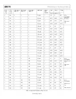
7:6
Data Delay Mode
00: Manual, no error correction
01: Manual, continuous error correction
10: automatic, one pass check
11: automatic, continuous pass check
00
5:3
Data Clock Delay
Data Clock delay control
000
03
Data Clock Delay
2:0 Data
Window
Delay
Window delay control
000
7:4
Sync Output Delay
0000
04
Synchronization
Delay
3:0 Sync
Window
Delay
0000
7
Sync Enable
0: LVDS and synchronization rceiver logic off
1: LVDS and synchronization rceiver logic on
0
6
Sync Driver Enable
0: LVDS driver off
1: LVDS driver on
0
05
Chip Sync and Data
Delay Control
5:3
DAC Clock Offset
0

