Programmer’s Model
2-12
Copyright © ARM Limited 2000. All rights reserved.
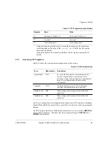
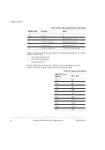
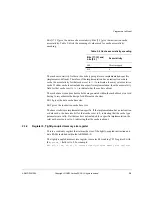
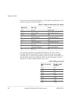
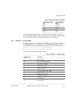
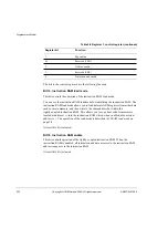
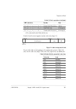
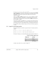
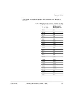
The bits in the control register have the following function.
Bit 19, Instruction RAM load mode
This bit controls the operation of the instruction RAM load mode.
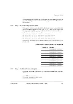
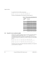
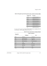
You can use the instruction RAM load mode for initializing the instruction RAM. The
instruction RAM load mode allows you to load data into ARM registers from either data
cache or main memory, and then write to the same address but within the
tightly-coupled instruction RAM. This allows you to copy boot code from memory
located at address
0x0
into the instruction RAM which, when enabled, also exists at
address
0x0
. The operation of the load mode is described in I-SRAM load mode on
At reset this bit is cleared.
Bit 18, Instruction RAM enable
This bit controls operation of the tightly-coupled instruction RAM. When the
instruction RAM is enabled, all instruction and data accesses to the instruction RAM
address range access the instruction RAM.
At reset this bit is cleared.
7
Big-endian
6:3
Reserved (SBO)
2
DCache enable
1
Reserved (SBZ)
0
Protection unit enable
Table 2-9 Register 1, control register (continued)
Register bit
Function
Summary of Contents for ARM946E-S
Page 1: ...ARM DDI 0155A ARM946E S Technical Reference Manual ...
Page 6: ...vi Copyright ARM Limited 2000 All rights reserved ARM DDI 0155A 04 Limited Confidential ...
Page 54: ...Programmer s Model 2 34 Copyright ARM Limited 2000 All rights reserved ARM DDI 0155A ...
Page 70: ...Caches 3 16 Copyright ARM Limited 2000 All rights reserved ARM DDI 0155A ...
Page 78: ...Protection Unit 4 8 Copyright ARM Limited 2000 All rights reserved ARM DDI 0155A ...
Page 112: ...Coprocessor Interface 7 14 Copyright ARM Limited 2000 All rights reserved ARM DDI 0155A ...

