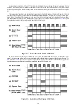
20
converter via data lines A
0
through A
6
. The data strobe output then goes low, and the memory full lamp is
extinguished.
If the operator types slower than the data transmission rate, the
ENABLE
signal is returned to the
encoder IC almost instantaneously, so the memory full light is energized only momentarily and therefore
does not emit a noticeable flash. On the other hand, if a new character is typed when the storage buffer is
full, the lamp will remain lit until the buffer is free, warning the operator that the storage capability of the
keyboard will be exceeded by additional keystrokes.
4.5 ROM Code Converter
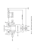
The seven ASCII code bits from the keyboard encoder are coupled to the input of a 2048-bit read-only
memory (ROM), shown with its control logic in Figure 8.4. The ROM is preprogrammed to store both the
Baudot and the Morse code equivalents of each ASCII character. An eighth bit, derived from the mode
switch via the identifier control circuit, indicates whether the Morse or the Baudot code is to be produced.
This bit is supplied to the ROM in parallel with the seven bits from the encoder. Together, these eight bits
form the address code fed to the ROM's input.
Each time a character code is fed to the ROM address inputs, a particular eight-bit storage location in the
memory is accessed. The data word stored there is either the Baudot or the Morse equivalent of the input
(address) word, depending on the state of the eighth bit. The stored bit pattern appears at the ROM outputs
in parallel. Thus, the input character is, in effect, converted from ASCII code to the bit pattern required for
Baudot or Morse transmission
In the RTTY mode, only five of the ROM output bits, D
1
through D
5
, are used to represent a particular
character. The other three control the RTTY character counter and the automatic case-change circuitry. If
the character to be transmitted is in the shifted case (that is, if it requires that the receiving printer be in
figures case), the D
0
bit of the ROM output will be high. Fed to the input of the case change flip-flop (Figure
8.5-A6), the bit causes the flip-flop to change states if the preceding character was in letters case. The
keyboard then transmits a figures-shift code before producing the current character. Likewise, if the current
character is in letters case, but the preceding one was in figures case, the D
0
bit will be low and the letters-
shift code will be sent. If two successive characters are in the same case, the D
0
bit does not change, and
no case-shift code is transmitted.
The D
6
and D
7
bits control the RTTY character counter (Figure 8.9). This counter keeps track of the
number of printing characters transmitted in sequence and lights a warning lamp when the end of the line is
approached, signaling the operator to transmit a carriage return and linefeed before proceeding. However,
not all characters result in printed output at the receiving end – some, such as the blank, do not print, and
thus do not add to the length of the line
. The character counter must therefore be instructed not to count
such characters. The D
7
bit of the ROM output is high for each non-printing character, disabling the
character counter.
When a carriage return is sent, the character counter must be reset for the start of a new line. The sixth
bit, D
6
, of the ROM output is low for this character only. The inverted D
6
signal is applied to the character
counter flip-flop reset terminals, returning the counter to the zero state when a carriage return is produced.
No case-change code is produced when a non-printing character is sent,as the D
7
line is high and the
case change flip-flop is therefore unable to respond the state of the D
0
bit.
4.6 Storage Buffer
The ROM output character contains the data eventually fed to the shift register, where it is converted
from parallel to serial form. Before it reaches the shift register, however, it enters a buffer storage register,
shown in Figure 8.4. If the shift register is busy producing a character when the code for the new character
appears at the ROM output, the new code will be stored in the buffer until the shift register has completed
its cycle and is ready to accept fresh input data.
Table 4.3 in Section 4.18 lists the ROM output code for each character.
Summary of Contents for DKB-2010
Page 1: ......
Page 20: ...18...
Page 39: ...37 Table 4 3 ROM Converter Input and Output Codes...
Page 52: ...50 Figure 6 1 Logic Circuit Board Test Points...
Page 53: ...51 Figure 6 2 Keyswitch Circuit Board Test Points...
Page 54: ...52 Figure 6 3 Power Supply Circuit Board Test Points...
Page 57: ...55 Table 6 4 DKB 2010 Wire List...
Page 63: ...61...
Page 64: ...62...
Page 65: ...63...
Page 67: ...65...
Page 69: ...67...
Page 71: ...69...
Page 73: ...71...
Page 75: ...73...
Page 77: ...75...
Page 79: ...77...
Page 81: ...79...
Page 83: ...81...
Page 85: ...83...
Page 87: ...85...
Page 89: ...87...
Page 91: ...89...
Page 92: ...90...
Page 93: ...91...
Page 94: ...92...
Page 95: ...93...
Page 96: ...A1 EXTENDED MEMORY OPTION FOR THE DKB 2010 KEYBOARD INSTRUCTION MANUAL...
Page 100: ...A5...
Page 101: ...A6...


