Rev. 1.50
11�
����st ��� �01�
Rev. 1.50
119
����st ��� �01�
HT66F0175/HT66F0185
A/D Flash MCU with EEPROM
HT66F0175/HT66F0185
A/D Flash MCU with EEPROM
A/D Converter Control Registers – SADC0, SADC1, SADC2, ACERL
To control the function and operation of the A/D converter, three control registers known as SADC0,
SADC1 and SADC2 are provided. These 8-bit registers define functions such as the selection of
which analog channel is connected to the internal A/D converter, the digitised data format, the
A/D clock source as well as controlling the start function and monitoring the A/D converter busy
status. As these devices contain only one actual analog to digital converter hardware circuit, each
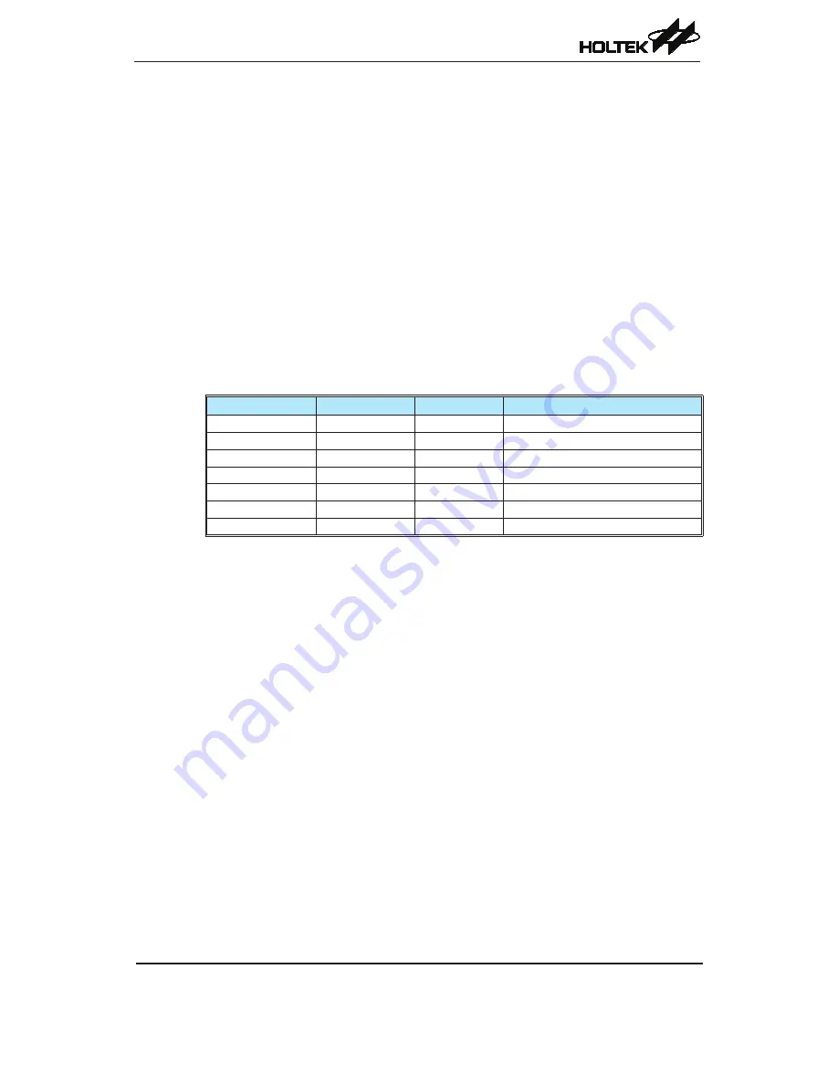
of the external and internal analog signals must be routed to the converter. The SACS2~SACS0
bits in the SADC0 register are used to determine which external channel input is selected to be
converted. The SAINS2~SAINS0 bits in the SADC1 register are used to determine that the analog
signal to be converted comes from the internal analog signal or external analog channel input. If the
SAINS2~SAINS0 bits are set to “000” or “100”, the external analog channel input will be selected
to be converted and the SACS2~SACS0 bits can deternine which external channel is selected to
be converted. If the SAINS2~SAINS0 bits are set to any other values except “000” and “100”, one
of the internal analog signals can be selected to be converted. The internal analog signals can be
derived from the A/D converter supply power, V
DD
, or internal reference voltage, V
R
, with a specific
ratio of 1, 1/2 or 1/4. If the internal analog signal is selected to be converted, the external channel
signal input will automatically be switched off to avoid the signal contention.
SAINS [2:0]
SACS [2:0]
Input Signals
Description
000� 100
000~111
�N0~�N�
External channel analo� inp�t
001
xxx
V
DD
�/D converter power s�pply volta�e
010
xxx
V
DD
/�
�/D converter power s�pply volta�e/�
011
xxx
V
DD
/4
�/D converter power s�pply volta�e/4
101
xxx
V
R
Internal reference volta�e
110
xxx
V
R
/�
Internal reference volta�e/�
111
xxx
V
R
/4
Internal reference volta�e/4
A/D Converter Input Signal Selection
The analog input pin function selection bits in the ACERL register determine which pins on I/O
Ports are used as external analog channels for the A/D converter input and which pins are not to be
used as the A/D converter input. When the pin is selected to be an A/D input, its original function
whether it is an I/O or other pin-shared functions will be removed. In addition, any internal pull-
high resistor connected to the pin will be automatically removed if the pin is selected to be an A/D
converter input.


