Rev. 1.50
66
����st ��� �01�
Rev. 1.50
6�
����st ��� �01�
HT66F0175/HT66F0185
A/D Flash MCU with EEPROM
HT66F0175/HT66F0185
A/D Flash MCU with EEPROM
I/O Port Control Registers
Each Port has its own control register, known as PAC~PDC, which controls the input/output
configuration. With this control register, each I/O pin with or without pull-high resistors can be
reconfigured dynamically under software control. For the I/O pin to function as an input, the
corresponding bit of the control register must be written as a “1”. This will then allow the logic state
of the input pin to be directly read by instructions. When the corresponding bit of the control register
is written as a “0”, the I/O pin will be setup as a CMOS output. If the pin is currently setup as an
output, instructions can still be used to read the output register.
However, it should be noted that the program will in fact only read the status of the output data latch
and not the actual logic status of the output pin.
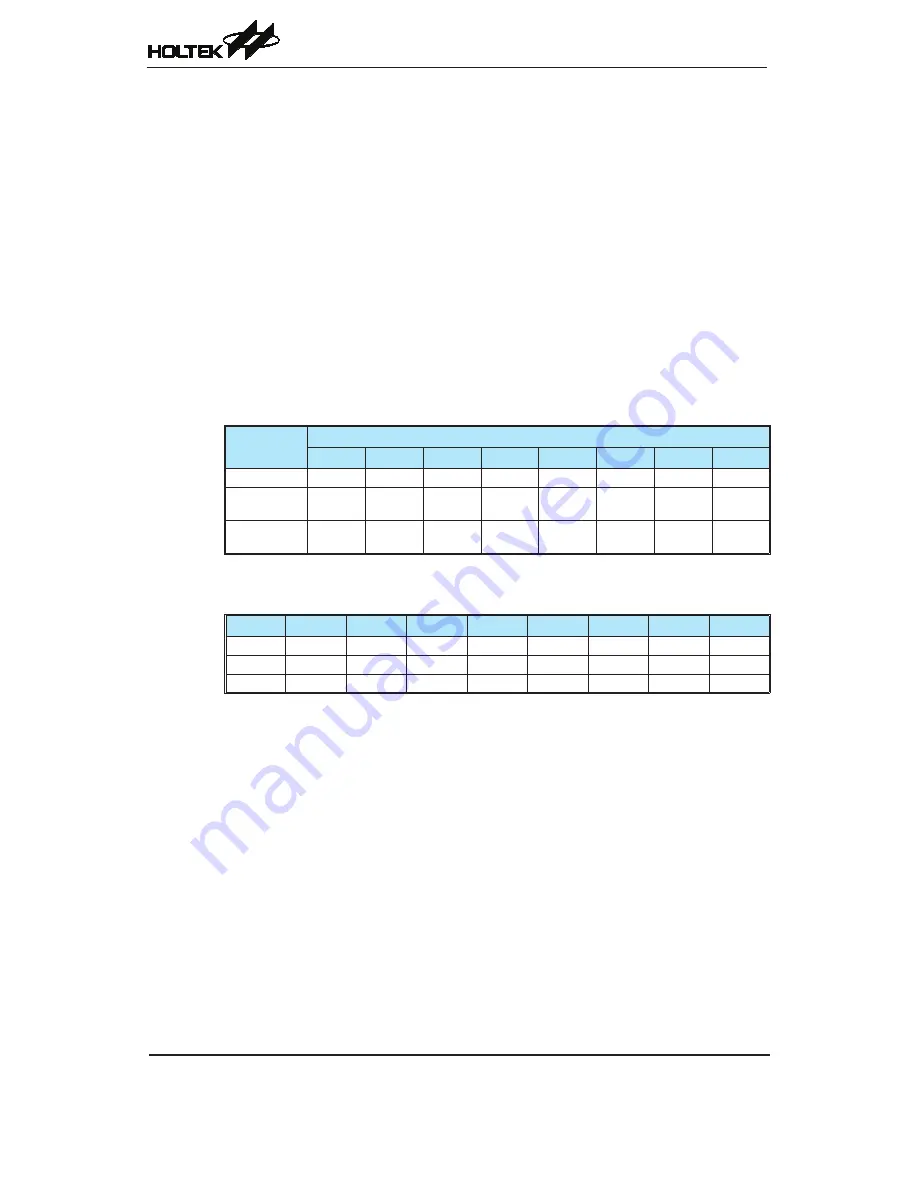
I/O Port Source Current Control
These devices support different source current driving capability for each I/O port. With the
corresponding selection register, SLEDC0 and SLEDC1, each I/O port can support four levels of the
source current driving capability. Users should refer to the D.C. characteristics section to select the
desired source current for different applications.
Register
Name
Bit
7
6
5
4
3
2
1
0
SLEDC0
PBPS3
PBPS�
PBPS1
PBPS0
P�PS3
P�PS�
P�PS1
P�PS0
SLEDC1
(HT66F01�5)
—
—
—
—
PCPS3
PCPS�
PCPS1
PCPS0
SLEDC1
(HT66F01�5)
—
—
PDPS1
PDPS0
PCPS3
PCPS�
PCPS1
PCPS0
I/O Port Source Current Control Registers List
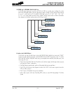
SLEDC0 Register
Bit
7
6
5
4
3
2
1
0
Name
PBPS3
PBPS�
PBPS1
PBPS0
P�PS3
P�PS�
P�PS1
P�PS0
R/W
R/W
R/W
R/W
R/W
R/W
R/W
R/W
R/W
POR
0
1
0
1
0
1
0
1
Bit 7~6
PBPS3~PBPS2
: PB6~PB4 source current selection
00: source current = Level 0 (min.)
01: source current = Level 1
10: source current = Level 2
11: source current = Level 3 (max.)
Bit 5~4
PBPS1~PBPS0
: PB3~PB0 source current selection
00: source current = Level 0 (min.)
01: source current = Level 1
10: source current = Level 2
11: source current = Level 3 (max.)
Bit 3~2
PAPS3~PAPS2
: PA7~PA4 source current selection
00: source current = Level 0 (min.)
01: source current = Level 1
10: source current = Level 2
11: source current = Level 3 (max.)
Bit 1~0
PAPS1~PAPS0
: PA3~PA0 source current selection
00: source current = Level 0 (min.)
01: source current = Level 1
10: source current = Level 2
11: source current = Level 3 (max.)


