EXTERNAL BUS
14-22
14.2.4
Bus and Control Signals During Recovery and Idle States
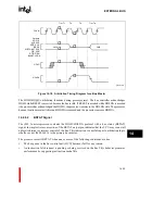
Valid bus transactions are bounded by ADS going active at the beginning of Ta states and BLAST
going inactive at the beginning of Tr states. During Tr and Ti states, bus and control pin logic
levels are defined in such a way as to avoid unnecessary pin transitions that waste power. In all
cases, the bus and control pins are completely quiet for instruction fetches and data loads that are
cache hits.
If the last bus cycle is a read, the address/data bus floats during all Tr states. If the last bus cycle is
a write, the address/data bus freezes during Tr states. The processor drives control pins such as
ALE, ADS, BLAST and DEN to their inactive states during Tr. Byte enables BE3:0 are always
driven to logic high during Tr, even when the processor uses them under alternate definitions.
Outputs without clearly defined active/inactive states such as A3:2, WIDTH/HLTD1:0, D/C, W/R
and DT/R freeze during Tr.
When the bus enters the Ti state, the bus and control pins will likewise freeze to inactive states.
The exact states of the address/data pins depend on how the processor enters the Ti state. If the
processor enters Ti from a Tr ending a write cycle, the processor continues driving data on
AD31:0. If the processor enters Ti from a read cycle or from a Th state, AD31:4 will be driven
with the upper 28 bits of the read address. AD3:2 will be driven identically as A3:2 (the word
address of the last read transfer). The processor will usually drive AD1:0 with the last SIZE infor-
mation. In cases where the core cancels a previously issued bus request, AD1:0 are indeterminate.
14.2.5
Data Alignment
The i960 Jx microprocessor’s Bus Control Unit (BCU) directly supports both big-endian and
little-endian aligned accesses. The processor also transparently supports both big-endian and
little-endian unaligned accesses but with reduced performance. Unaligned accesses are broken down
into a series of aligned accesses with the assistance of microcode executing on the processor.
Alignment rules for loads and stores are based on address offsets from natural data boundaries.
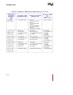
Table 14-5
lists the natural boundaries for the various data widths and
Table 14-6
through 14-8 list all
possible combinations of bus accesses resulting from aligned and unaligned requests.
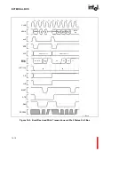
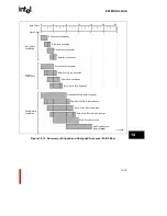
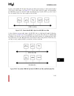
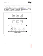
Figure 14-13
and
Figure 14-14
also depict all the combinations for 32-bit buses.
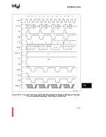
Figure 14-15
is a functional
waveform for a series of four accesses resulting from a misaligned double word read request.
The fault configuration word in the Process Control Block (PRCB), can configure the processor to
handle unaligned accesses non-transparently by generating an OPERATION.UNALIGNED fault after
executing any unaligned access. See
section 12.3.1.2, “Process Control Block (PRCB)” (pg. 12-16)
.
Summary of Contents for i960 Jx
Page 1: ...Release Date December 1997 Order Number 272483 002 i960 Jx Microprocessor Developer s Manual ...
Page 24: ......
Page 25: ...1 INTRODUCTION ...
Page 26: ......
Page 35: ...2 DATA TYPES AND MEMORY ADDRESSING MODES ...
Page 36: ......
Page 46: ......
Page 47: ...3 PROGRAMMING ENVIRONMENT ...
Page 48: ......
Page 73: ...4 CACHE AND ON CHIP DATA RAM ...
Page 74: ......
Page 85: ...5 INSTRUCTION SET OVERVIEW ...
Page 86: ......
Page 111: ...6 INSTRUCTION SET REFERENCE ...
Page 112: ......
Page 233: ...7 PROCEDURE CALLS ...
Page 234: ......
Page 256: ......
Page 257: ...8 FAULTS ...
Page 258: ......
Page 291: ...9 TRACING AND DEBUGGING ...
Page 292: ......
Page 309: ...10 TIMERS ...
Page 310: ......
Page 324: ......
Page 325: ...11 INTERRUPTS ...
Page 326: ......
Page 369: ...12 INITIALIZATION AND SYSTEM REQUIREMENTS ...
Page 370: ......
Page 412: ......
Page 413: ...13 MEMORY CONFIGURATION ...
Page 414: ......
Page 429: ...14 EXTERNAL BUS ...
Page 430: ......
Page 468: ......
Page 469: ...15 TEST FEATURES ...
Page 470: ......
Page 493: ...A CONSIDERATIONS FOR WRITING PORTABLE CODE ...
Page 494: ......
Page 502: ......
Page 503: ...B OPCODES AND EXECUTION TIMES ...
Page 504: ......
Page 515: ...C MACHINE LEVEL INSTRUCTION FORMATS ...
Page 516: ......
Page 523: ...D REGISTER AND DATA STRUCTURES ...
Page 524: ......
Page 550: ......
Page 551: ...GLOSSARY ...
Page 552: ......
Page 561: ...INDEX ...
Page 562: ......
Page 578: ......


