CACHE AND ON-CHIP DATA RAM
4-7
4
4.5.2
Multi-Word Data Accesses that Partially Hit the Data Cache
The following applies only when data caching is enabled for an access.
For a multi-word load access (
ldl
,
ldt
,
ldq
) in which none of the requested words hit the data cache,
an external bus transaction is started to acquire all the words of the access.
For a multi-word load access that partially hits the data cache, the processor may either:
•
Load or reload all words of the access (even those that hit) from the external bus
•
Load only missing words from the external bus and interleave them with words found in the data cache
The multi-word alignment determines which of the above methods is used:
•
Naturally aligned multi-word accesses cause all words to be reloaded
•
An unaligned multi-word access causes only missing words to be loaded
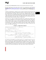
When any words accessed by a
ldl
,
ldt
, or
ldq
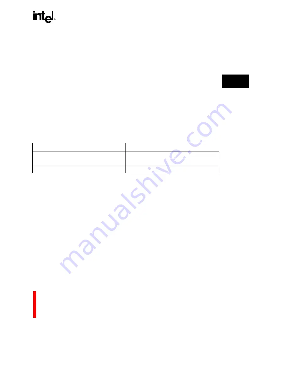
instruction miss the data cache, every word accessed
by that load instruction is updated in the cache.
In each case, the external bus accesses used to acquire the data may consist of none, one, or several
burst accesses based on the alignment of the data and the bus-width of the memory region that
contains the data. See
CHAPTER 14, EXTERNAL BUS
for more details.
A multi-word load access that completely hits in the data cache does not cause external bus accesses.
For a multi-word store access (
stl
,
stt
,
stq
) an external bus transaction is started to write all words
of the access regardless when any or all words of the access hit the data cache. External bus
accesses used to write the data may consist of either one or several burst accesses based on data
alignment and the bus-width of the memory region that receives the data. (See
CHAPTER 14,
EXTERNAL BUS
for more details.) The cache is also updated accordingly as described earlier in
this chapter.
Table 4.1.
Load Instruction
Number of Updated Words
ldq
4 words
ldt
3 words
ldl
2 words
Summary of Contents for i960 Jx
Page 1: ...Release Date December 1997 Order Number 272483 002 i960 Jx Microprocessor Developer s Manual ...
Page 24: ......
Page 25: ...1 INTRODUCTION ...
Page 26: ......
Page 35: ...2 DATA TYPES AND MEMORY ADDRESSING MODES ...
Page 36: ......
Page 46: ......
Page 47: ...3 PROGRAMMING ENVIRONMENT ...
Page 48: ......
Page 73: ...4 CACHE AND ON CHIP DATA RAM ...
Page 74: ......
Page 85: ...5 INSTRUCTION SET OVERVIEW ...
Page 86: ......
Page 111: ...6 INSTRUCTION SET REFERENCE ...
Page 112: ......
Page 233: ...7 PROCEDURE CALLS ...
Page 234: ......
Page 256: ......
Page 257: ...8 FAULTS ...
Page 258: ......
Page 291: ...9 TRACING AND DEBUGGING ...
Page 292: ......
Page 309: ...10 TIMERS ...
Page 310: ......
Page 324: ......
Page 325: ...11 INTERRUPTS ...
Page 326: ......
Page 369: ...12 INITIALIZATION AND SYSTEM REQUIREMENTS ...
Page 370: ......
Page 412: ......
Page 413: ...13 MEMORY CONFIGURATION ...
Page 414: ......
Page 429: ...14 EXTERNAL BUS ...
Page 430: ......
Page 468: ......
Page 469: ...15 TEST FEATURES ...
Page 470: ......
Page 493: ...A CONSIDERATIONS FOR WRITING PORTABLE CODE ...
Page 494: ......
Page 502: ......
Page 503: ...B OPCODES AND EXECUTION TIMES ...
Page 504: ......
Page 515: ...C MACHINE LEVEL INSTRUCTION FORMATS ...
Page 516: ......
Page 523: ...D REGISTER AND DATA STRUCTURES ...
Page 524: ......
Page 550: ......
Page 551: ...GLOSSARY ...
Page 552: ......
Page 561: ...INDEX ...
Page 562: ......
Page 578: ......


