657
Chapter 16
Clocked Serial Interface B (CSIB)
User’s Manual U16580EE3V1UD00
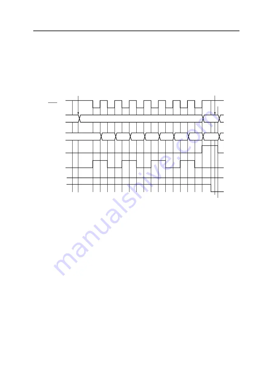
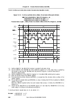
16.4.3 Single transfer mode (master mode, reception mode)
Figure 16-11:
Single Transfer Mode (Master Mode, Reception Mode)
MSB First (CBnDIR Bit of CBnCTL0 Register = 0),
CBnCKP Bit of the CBnCTL1 Register = 0,
CBnDAP Bit of the CBnCTL1 Register = 0,
Transfer Data Length = 8 Bits (CSnCL3 to CBnCL0 Bits of CBnCTL2 Register = 0000B)
<1> Set the CBnCTL1 and CBnCTL2 registers to specify the transfer mode.
<2> Set the CBnRXE bit of the CBnCTL0 register to 1 at the same time as specifying the transfer
mode using the CBnDIR bit of the CBnCTL0 register, to set the reception enabled status.
<3> Set the CBnPWR bit of the CBnCTL0 register to 1 to enable CSIB operating clock supply.
<4> Perform a dummy read of the CBnRX register (reception start trigger).
<5> The reception complete interrupt (INTCBnR) is output, notifying the CPU that reading the CBnRX
(CBnRXL) register is possible.
<6> Clear the CBnSCE bit of the CBnCTL0 register to 0 to set the reception end data status.
<7> Read the CBnRX register before clearing the CBnPWR bit to 0.
<8> Check that the CBnTSF bit of the CBnSTR register is 0 and clear the CBnPWR bit to 0 to stop
clock supply to CSIB (end of reception).
To continue transfer, repeat steps <4> and <5> before <6>. (At this time, <4> is not a dummy read, but
a receive data read combined with the reception trigger.)
Remarks: 1.
The processing of steps <2> and <3> can be set simultaneously.
2.
μ
PD70F3187:
n = 0, 1
μ
PD70F3447:
n = 0
(AAH)
1
0
1
1
0
1
ABH
56H
ADH
5AH
B5H
6AH
D5H
AAH
55H (receive data)
SCKBn pin
CBnRX
register
CBnRX register read (55H)
Shift
register n
CBnSCE bit
INTCBnR
signal
SIBn pin
SOBn pin
0
0
L
<1>
<2>
<3>
<4>
<5>
<6>
<8>
<7>
CBnRX register read (AAH)
AAH
00H
00H
Summary of Contents for V850E/PH2
Page 6: ...6 Preface User s Manual U16580EE3V1UD00...
Page 16: ...16 User s Manual U16580EE3V1UD00...
Page 28: ...28 User s Manual U16580EE3V1UD00...
Page 32: ...32 User s Manual U16580EE3V1UD00...
Page 84: ...84 Chapter 2 Pin Functions User s Manual U16580EE3V1UD00 MEMO...
Page 144: ...144 Chapter 3 CPU Functions User s Manual U16580EE3V1UD00 MEMO...
Page 192: ...192 Chapter 5 Memory Access Control Function PD70F3187 only User s Manual U16580EE3V1UD00 MEMO...
Page 312: ...312 Chapter 9 16 Bit Timer Event Counter P User s Manual U16580EE3V1UD00 MEMO...
Page 534: ...534 Chapter 11 16 bit Timer Event Counter T User s Manual U16580EE3V1UD00...
Page 969: ...969 Chapter 20 Port Functions User s Manual U16580EE3V1UD00 MEMO...
Page 970: ...970 Chapter 20 Port Functions User s Manual U16580EE3V1UD00...
Page 976: ...976 Chapter 22 Internal RAM Parity Check Function User s Manual U16580EE3V1UD00 MEMO...
Page 984: ...984 Chapter 23 On Chip Debug Function OCD User s Manual U16580EE3V1UD00 MEMO...
Page 1006: ...1006 Chapter 24 Flash Memory User s Manual U16580EE3V1UD00 MEMO...
Page 1036: ...1036 Chapter 27 Recommended Soldering Conditions User s Manual U16580EE3V1UD00 MEMO...
Page 1046: ...1046 Appendix A Index User s Manual U16580EE3V1UD00 MEMO...
Page 1052: ...1052 User s Manual U16580EE3V1UD00...
Page 1053: ......


