707
Chapter 17
Clocked Serial Interface 3 (CSI3)
User’s Manual U16580EE3V1UD00
17.5.11 Transmission
mode
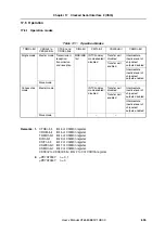
The transmission mode is set when the CTXEn bit of the CSIM3n register is set to 1 and the CRXEn bit
is cleared to 0. In this mode, transmission is started by a trigger that writes transmit data to the SFDB3n
register or sets the CTXEn bit to 1 when transmit data is in the SFDB3n register (n = 0, 1). Even in the
single mode (TRMDn bit of the CSIM3n register = 0), whether the SIRB3n or SIO3n register is empty
has nothing to do with starting transmission. The value input to the SI3n pin during transmission is
latched in the shift register (SIO3n) but is not transferred to the SIRB3n and CSIBUFn registers at the
end of transmission.
The transmission/reception completion interrupt (INTC3n) occurs immediately after data is sent out
from the SIO3n register.
17.5.12 Reception
mode
The reception mode is set when the CTXEn bit of the CSIM3n register is cleared to 0 and CRXEn bit is
set to 1. In this mode, reception is started by using the processing of writing dummy data to the
SFDB3n register as a trigger (n = 0, 1). In the single mode (TRMDn bit of the CSIM3n register = 0),
however, the condition of starting reception includes that the SIRB3n or SIO3n register is empty. (If
reception to the SIO3n register is completed when the previously received data is held in the SIRB3n
register without being read, the previously received data is read from the SIRB3n register and the wait
status continues until the SIRB3n register becomes empty.)
The SO3n pin outputs a low level.
The transmission/reception completion interrupt (INTC3n) occurs immediately after receive data is
transferred from the SIO3n register to the SIRB3n register.
17.5.13 Transmission/reception
mode
The transmission/reception mode is set when both the CTXEn and CRXEn bits of the CSIM3n register
are set to 1. In this mode, transmission/reception is started by using the processing to write transmit
data to the SFDB3n register as a trigger (n = 0, 1). In the single mode (TRMDn bit of the CSIM3n
register = 0), however, the condition of starting transmission/reception includes that the SIRB3n or
SIO3n register is empty. (If reception to the SIO3n register is completed when the previously received
data is held in the SIRB3n register without being read, the previously received data is read from the
SIRB3n register and the wait status continues until the SIRB3n register becomes empty.)
Remark:
μ
PD70F3187:
n = 0, 1
μ
PD70F3447:
n = 0
Summary of Contents for V850E/PH2
Page 6: ...6 Preface User s Manual U16580EE3V1UD00...
Page 16: ...16 User s Manual U16580EE3V1UD00...
Page 28: ...28 User s Manual U16580EE3V1UD00...
Page 32: ...32 User s Manual U16580EE3V1UD00...
Page 84: ...84 Chapter 2 Pin Functions User s Manual U16580EE3V1UD00 MEMO...
Page 144: ...144 Chapter 3 CPU Functions User s Manual U16580EE3V1UD00 MEMO...
Page 192: ...192 Chapter 5 Memory Access Control Function PD70F3187 only User s Manual U16580EE3V1UD00 MEMO...
Page 312: ...312 Chapter 9 16 Bit Timer Event Counter P User s Manual U16580EE3V1UD00 MEMO...
Page 534: ...534 Chapter 11 16 bit Timer Event Counter T User s Manual U16580EE3V1UD00...
Page 969: ...969 Chapter 20 Port Functions User s Manual U16580EE3V1UD00 MEMO...
Page 970: ...970 Chapter 20 Port Functions User s Manual U16580EE3V1UD00...
Page 976: ...976 Chapter 22 Internal RAM Parity Check Function User s Manual U16580EE3V1UD00 MEMO...
Page 984: ...984 Chapter 23 On Chip Debug Function OCD User s Manual U16580EE3V1UD00 MEMO...
Page 1006: ...1006 Chapter 24 Flash Memory User s Manual U16580EE3V1UD00 MEMO...
Page 1036: ...1036 Chapter 27 Recommended Soldering Conditions User s Manual U16580EE3V1UD00 MEMO...
Page 1046: ...1046 Appendix A Index User s Manual U16580EE3V1UD00 MEMO...
Page 1052: ...1052 User s Manual U16580EE3V1UD00...
Page 1053: ......

