688
Chapter 17
Clocked Serial Interface 3 (CSI3)
User’s Manual U16580EE3V1UD00
(6)
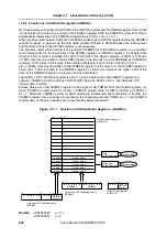
CSIBUF status register 3n (SFA3n)
The SFA3n register indicates the status of the CSIBUFn register or the transfer status.
This register can be read or written in 8-bit or 1-bit units (however, bits 6 to 0 can only be read.
They do not change even if they are written).
Reset input clears the register to 20H.
Cautions: 1. Reading the SFA3n register is prohibited when the CSICAEn bit of the CSIM3n
register is cleared (0).
2. Because the values of the SFFULn, SFEMPn, CSOTn, and SFPn3 to SFPn0 bits
may change at any time during transfer, their values during transfer may differ
from the actual values. Especially, use the CSOTn bit independently (do not use
this bit in relation with the other bits). To detect the end of transfer by the SFA3n
register, check to see if the SFEMPn bit is 1 after the data to be transferred has
been written to the CSIBUFn register.
3. If the SFA3n register is read immediately after data has been written to the
SFDB3n and SFDB3nL registers, the values of the SFFULn, SFEMPn, and SFPn3
to SFPn0 bits do not change in time.
4. If the SFA3n register is read before the SFFULn bit is set to 1 and the 17th data is
written, the CSIBUFn overflow interrupt (INTC3nOVF) is generated.
Figure 17-7:
CSIBUF Status Register 3n (SFA3n)(1/3)
Note:
Not available on µPD70F3447
Remark:
μ
PD70F3187:
n = 0, 1
μ
PD70F3447:
n = 0
After reset:
00H
R/W
Address:
SFA30 FFFFFD48H,
SFA31 FFFFFD68H
Note
7
6
5
4
3
2
1
0
SFA3n
FPCLRn
SFFULn
SFEMPn
CSOTn
SFPn3
SFPn2
SFPn1
SFPn0
FPCLRn
CSIBUFn Pointer Clear Operation
0
No operation
1
Clear all CSIBUFn pointers
Cautions: 1. This bit is always 0 when it is read.
2. If 1 is written to the FPCLRn bit in the middle of transfer, transfer is
aborted. Because all the CSIBUFn pointers are cleared to 0, the
remaining data in the CSIBUFn register is ignored.
If 1 is written to the FPCLRn bit, be sure to read the SFA3n register to
check to see if all the CSIBUFn pointers have been correctly cleared
to 0 (SFFULn bit = 0, SFEMPn bit = 1, SFPn3 to SFPn0 bits = 0000B).
Nothing happens even if 0 is written to the FPCLRn bit.
Summary of Contents for V850E/PH2
Page 6: ...6 Preface User s Manual U16580EE3V1UD00...
Page 16: ...16 User s Manual U16580EE3V1UD00...
Page 28: ...28 User s Manual U16580EE3V1UD00...
Page 32: ...32 User s Manual U16580EE3V1UD00...
Page 84: ...84 Chapter 2 Pin Functions User s Manual U16580EE3V1UD00 MEMO...
Page 144: ...144 Chapter 3 CPU Functions User s Manual U16580EE3V1UD00 MEMO...
Page 192: ...192 Chapter 5 Memory Access Control Function PD70F3187 only User s Manual U16580EE3V1UD00 MEMO...
Page 312: ...312 Chapter 9 16 Bit Timer Event Counter P User s Manual U16580EE3V1UD00 MEMO...
Page 534: ...534 Chapter 11 16 bit Timer Event Counter T User s Manual U16580EE3V1UD00...
Page 969: ...969 Chapter 20 Port Functions User s Manual U16580EE3V1UD00 MEMO...
Page 970: ...970 Chapter 20 Port Functions User s Manual U16580EE3V1UD00...
Page 976: ...976 Chapter 22 Internal RAM Parity Check Function User s Manual U16580EE3V1UD00 MEMO...
Page 984: ...984 Chapter 23 On Chip Debug Function OCD User s Manual U16580EE3V1UD00 MEMO...
Page 1006: ...1006 Chapter 24 Flash Memory User s Manual U16580EE3V1UD00 MEMO...
Page 1036: ...1036 Chapter 27 Recommended Soldering Conditions User s Manual U16580EE3V1UD00 MEMO...
Page 1046: ...1046 Appendix A Index User s Manual U16580EE3V1UD00 MEMO...
Page 1052: ...1052 User s Manual U16580EE3V1UD00...
Page 1053: ......


