SERIES AP440 ACROPACK
USER
’S MANUAL
Acromag, Inc. Tel: 248-295-0310
- 37 - http://www.acromag.com
- 37 -
www.acromag.com
4.0 THEORY OF OPERATION
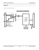
This section provides a description of the basic functionality of the circuitry
used on the board. Refer to the Block Diagram shown in Figure 1, Appendix
B, as you review this material.
4.1 AcroPack 440 Operation
The AP440 is built around a digital FPGA chip that provides I/O interface and
configuration functions. This chip performs monitor and control functions of
up to 32 open-drain inputs. The FPGA also provides debounce control and
event sensing functions. The FPGA provides the control interface necessary
to operate the module.
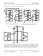
The field I/O interface to the carrier board is provided through connector P2
(refer to Table 2.1). Individual optocouplers for each channel isolate the
field from the control logic for the AP440. Channels are isolated from each
other in groups of eight. There are eight channels to a group or port.
Because the output lines of a single port share a common connection,
individual outputs are not isolated from each other within the same port.
However, separate port commons are provided to facilitate port-to-port
isolation.
Input optocouplers of this device are bipolar and accept voltages in three
ranges:
(4-18V),
(16-40V), and
(38-60V), DC or AC peak. The
optocouplers connect directly to the FPGA functioning as a controller that
provides the I/O read/write functionality, interrupt handling, and debounce
control.
4.2 PCIe Interface Logic
The PCIe bus interface logic is imbedded within the FPGA. This logic includes
support for PCIe commands, including: configuration read/write, and
memory read/write. In addition, the PCIe target interface uses a single 4K
base address register, and implements target abort, retry, and disconnect.
The AP440 logic also implements interrupt requests via the PCIe bus.
A FPGA device provides the control signals required to operate the board. It
decodes the selected addresses, control signals, and interrupt handling. It
also returns the acknowledgement messages required by the carrier/CPU
board per the PCIe specification. The program for the FGPA is stored in
separate Flash memory and loaded upon power-up.


