background image

SERIES IP1K110 INDUSTRIAL I/O PACK                                        RECONFIGURABLE DIGITAL I/O MODULE 
__________________________________________________________________________________________


- 11 - 

Acromag, Inc.  Tel:248-295-0310  Fax:248-624-9234  Email:solutions@acromag.com  

http://www.acromag.com


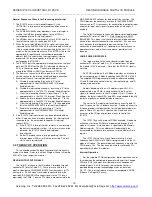
The address specified in the Memory Address register will be 

automatically incremented after the read or write cycle is 
completed.  Thus, when consecutive locations within the memory 
are accessed the Memory Address register need not be manually 
updated by software.  

 
Read or write accesses to this register require four wait 

states.  A software or hardware reset has no affect on this 
register. 

 
Memory Address Register (Write Only, 16H) 
 

The Memory Address register is used to point to one of 64K 

words in memory.  The 16 bits of this register are used to specify 
one of 64K words that can be accessed via a read or write to the 
Memory Data register.  Writing to this register is possible via 16-
bit data transfers only. 

 
The address specified in the Memory Address register will be 

automatically incremented after the read or write cycle to the 
Memory Data register is completed.  Thus, when consecutive 
locations within the memory are accessed the Memory Address 
register need not be manually incremented by software. 

 
A write access to this register requires one wait state.  A 

software or hardware reset will clear this register to zero. 
 

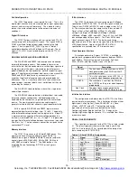
Clock Control Reg 1 (Read/Write) – (Base + 18H) 
 

      The Clock Control Register 1 is a 16-bit read/write register.  
This is used as part of the control for the Cypress CY22150 
Programmable Clock.  The register contains the following control 
bits as specified in the Cypress CY22150 spec sheet. 
 

Bit 

Data 

Bit 

Data 

D0 

DIV1N(0) 

D8 

Q(0) 

D1 

DIV1N(1) 

D9 

Q(1) 

D2 

DIV1N(2) 

D10 

Q(2) 

D3 

DIV1N(3) 

D11 

Q(3) 

D4 

DIV1N(4) 

D12 

Q(4) 

D5 

DIV1N(5) 

D13 

Q(5) 

D6 

DIV1N(6) 

D14 

Q(6) 

D7 

DIV1SRC 

D15 

PO 

A software or hardware reset will clear this register to zero. 


Clock Control Reg 2 (Read/Write) – (Base + 1AH) 
 

      The Clock Control Register 2 is a 16-bit read/write register.  
This is used as part of the control for the Cypress CY22150 
Programmable Clock.  The register contains the following control 
bits as specified in the Cypress CY22150 spec sheet. 
 

Bit 

Data 

Bit  

Data 

D0 

PB(0) 

D8 

PB(8) 

D1 

PB(1) 

D9 

PB(9) 

D2 

PB(2) 

D10 

Pump(0) 

D3 

PB(3) 

D11 

Pump(1) 

D4 

PB(4) 

D12 

Pump(2) 

D5 

PB(5) 

D13 

CLKSRC0 

D6 

PB(6) 

D14 

CLKSRC1 

D7 

PB(7) 

D15 

CLKSRC2 

A software or hardware reset will clear this register to zero. 


Clock Control Reg 3 (Read/Write) – (Base + 1DH)


      The Clock Control Register 3 is an 8-bit read/write register.  
This is used as part of the control for the Cypress CY22150 
Programmable Clock.  In this register only D0 (bit 0) and D7 (bit 
7) are required.  The other bits (D1-D6) are not used. 
 
      The value for D0 is zero if the carrier board provides an 8MHz 
clock to the FPGA.  D0 is logic high if the carrier board provides a 
32MHz signal to the FPGA.  D7 is an enable/disable signal for the 
CY22150 IC. Writing a ‘1’ to bit 7 will disable the clock generator 
chip, including the programming function.   Setting D7 to zero will 
allow for normal operation.  A software or hardware reset will 
clear this register to zero. 
 

Clock Trigger Register (Read/Write) – (Base + 1FH) 


The Clock Trigger Register is an 8-bit register.  To initiate 

programming of the Cypress CY22150 Programmable Clock, 
write a “1” to bit 0 of this register.  During programming bit 0 will 
remain logic high.  The programming process takes 
approximately 1.2ms to complete after the initial trigger.  A 
software or hardware reset has no affect on this register. 

 
Program Procedure to Set Clock Frequency 


At power up the programmable clock has no valid output.  

The clock can be programmed for an output frequency from  
250 KHz to 100 MHz.   The clock can be programmed at any time 
during device operation.  Program the clock using the following 
process. 
 
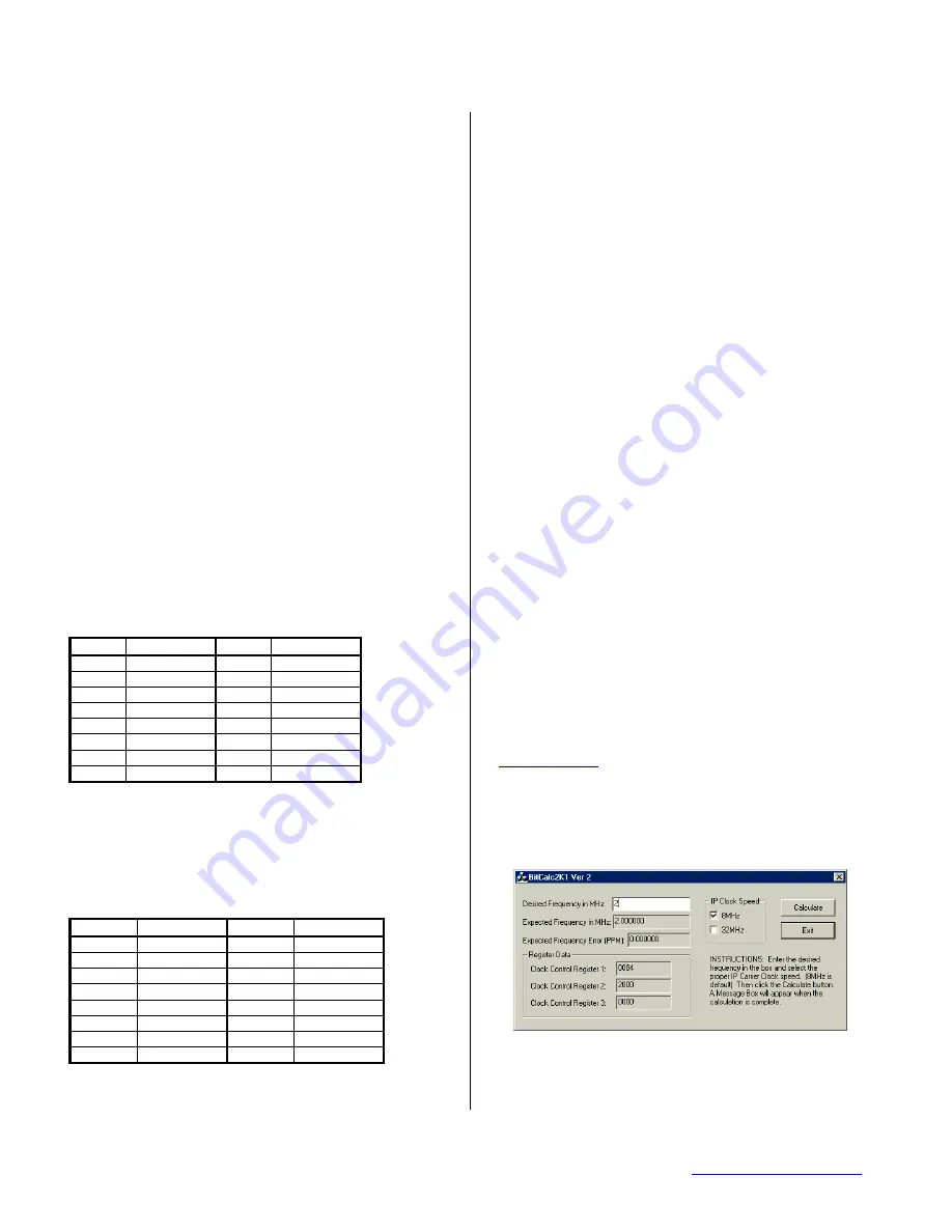
      The program words required for Clock Control Register 1, 2, 
and 3 can be calculated using a program provided by Acromag 
(BitCalc2K1 Version 2) supplied with the EDK.  Alternately, using 
the Clock Control Registers Data Maps and the CY22150 
specification sheet the necessary values can be calculated.  
Cypress has a program CyberClocks available to aid with 
calculations.  Note that the user will have to combine the 
individual variables into the control words as outlined in the 
register descriptions.  The CY22150 Specification Sheets and 
CyberClocks program are available from Cypress

 at 

www.cypress.com

 
      The reference frequency input to the Cypress CY22150 is the 
same as the carrier clock either 8MHz or 32MHz. 
 

Procedure 

1. 

Start the BitCalc2K1 Version 2 program, enter the desired 
frequency, and select the IP clock speed. 


2. 

Hit the Calculate Button. 

3. 

Write to the Clock Control Register 1 at base address plus 
an offset of 18H using the data provided by the program.   

4. 

Write to the Clock Control Register 2 at base address plus 
an offset of 1AH using the data provided by the program.   

Summary of Contents for IP1K110 Series

Page 1: ...NUAL ACROMAG INCORPORATED Tel 248 295 0310 30765 South Wixom Road Fax 248 624 9234 P O BOX 437 Wixom MI 48393 7037 U S A solutions acromag com Copyright 2004 2011 Acromag Inc Printed in the USA Data and specifications are subject to change without notice 8500 724 F11M004 retired ...

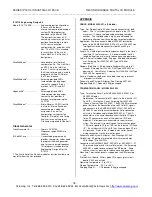
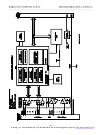
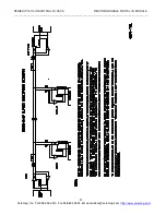
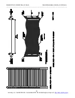
Page 2: ...6 PHYSICAL 16 ENVIRONMENTAL 17 EIA RS485 RS422 TRANSCEIVERS 17 TTL TRANSCEIVERS 17 INDUSTRIAL I O PACK COMPLIANCE IP1K110 ENGINEERING DESIGN KIT 17 18 APPENDIX 18 CABLE MODEL 5025 551 18 CABLE MODEL 5025 552 18 TRANSITION MODULE MODEL TRANS GP 19 DRAWINGS Page 4501 971 IP1K110 BLOCK DIAGRAM 20 4501 702 RS485 I O CONNECTIONS 21 4501 434 IP MECHANICAL ASSEMBLY 22 4501 462 CABLE 5025 550 NON SHIELDED...

Page 3: ...y be mounted on a 6U VMEbus carrier board or five units may be mounted on a PCI carrier board Local ID Each IP module has its own 8 bit ID information which is accessed via data transfers in the ID Read space 16 bit 8 bit I O Channel register Read Write is performed through D16 or D08 EO data transfer cycles in the IP module I O space High Speed Access times for all data transfer cycles are descri...

Page 4: ...s recommended that the board be visually inspected for evidence of mishandling prior to applying power The board utilizes static sensitive components and should only be handled at a static safe workstation CARD CAGE CONSIDERATIONS Refer to the specifications for loading and power requirements Be sure that the system power supplies are able to accommodate the power requirements of the carrier board...

Page 5: ...S485 RS422 communication distances are generally limited to less than 4000 feet To minimize transmission line problems all nodes connected to the cable must use minimum stub length connections The optimal configuration for the RS485 RS422 bus is a daisy chain connection from node 1 to node 2 to node 3 to node n The bus must form a single continuous path and the nodes in the middle of the bus must ...

Page 6: ... Thus download and configuration is implemented with no special hardware or cables An example program written in C and available from Acromag implements configuration of the IP1K110 over the IP bus The program requires the configuration file to be in the Intel Hex format Using the Altera MAX PLUS II software you can generate the required hex file as follows 1 In the MAX PLUS II Compiler choose the...

Page 7: ...codes Variable information includes unique information required for the module The IP1K110 ID space does not contain any variable e g unique calibration information ID space bytes are addressed using only the odd addresses in a 64 byte block on the Big Endian VMEbus Even addresses are used on the Little Endian PC ISA or PCI buses The IP1K110 ID space will read differently in configuration mode tha...

Page 8: ...sed in the Motorola 68000 and PowerPC microprocessor family and is the VMEbus convention In Big Endian the lower order byte is stored at odd byte addresses The Intel x86 family of microprocessors uses the opposite convention or Little Endian byte ordering Little Endian uses even byte addresses to store the low order byte As such use of the memory map for this module on a PC carrier board will requ...

Page 9: ...o or four channels while data direction of all TTL channels is controlled as a group of 8 channels Setting a bit high configures the data direction for the identified channels as output Setting the control bit low configures the corresponding channel s data direction for input The default power up state of these registers is logic low Thus all channels are configured as inputs on system reset or p...

Page 10: ...ster MSB LSB Data Bit 07 Data Bit 06 Data Bit 05 Data Bit 04 Data Bit 03 Data Bit 02 Data Bit 01 Data Bit 00 Ch07 Ch06 Ch05 Ch04 Ch03 Ch02 Ch01 Ch00 The unused upper 8 bits of this register are Not Used and will always read low 0 s for D16 accesses All bits are set to 0 following a reset which means that all interrupts are cleared Interrupt Polarity Registers Read Write Base 11H The Interrupt Pola...

Page 11: ...7 PB 7 D15 CLKSRC2 A software or hardware reset will clear this register to zero Clock Control Reg 3 Read Write Base 1DH The Clock Control Register 3 is an 8 bit read write register This is used as part of the control for the Cypress CY22150 Programmable Clock In this register only D0 bit 0 and D7 bit 7 are required The other bits D1 D6 are not used The value for D0 is zero if the carrier board pr...

Page 12: ...el s interrupt is serviced The response time of the input channels should also be considered when calculating this bandwidth The total response time is the sum of the input buffer response time plus the interrupt logic circuit response time and this time must pass before another interrupt condition will be recognized The Interrupt Input Response Time is specified in section 6 The following program...

Page 13: ...UT SIGNALS The field I O interface to the IP module is provided through connector P2 refer to Table 2 1 These pins are tied to the inputs and outputs of EIA RS485 RS422 line transceivers or TTL transceivers RS485 signals received are converted from the required EIA RS485 RS422 voltages signals to the TTL levels required by the FPGA Likewise TTL signals are converted to the EIA RS485 RS422 voltages...

Page 14: ...entional TTL level Memory Interface The IP1K110 interfaces to a 64K word SRAM device This memory interface utilizes the address signals RAMa1 to RAMa16 data signals RAMd0 to RAMd15 and the read write control signals nWE_RAM nBLE_RAM nBHE_RAM and nOE_RAM as listed in Table 4 1 The RAM device is the Integrated Device Technology IDT71016 or the Cypress Cy7C1021 IP Bus Interface The IP1K110 interfaces...

Page 15: ...utput 62 DIO0 Bi Dir 63 DIO1 Bi Dir 64 DIO2 Bi Dir 65 DIO3 Bi Dir 66 VCCIO 3 3Volts 67 DIO4 Bi Dir 68 DIO5 Bi Dir 69 DIO6 Bi Dir 70 DIO7 Bi Dir 71 DIO8 Bi Dir 72 VCCINT 2 5Volts 73 DIO9 Bi Dir Pin Signal I O 74 DIO10 Bi Dir 75 DIO11 Bi Dir 76 GND GND 77 VCC_CKLK 2 5Volts 78 nBS0 Input IP Bus 79 IP CLK GCLK1 IP Module Clock 80 nBS1 Input IP Bus 81 GND_CKLK GND 82 GND GND 83 DIO12 Bi Dir 84 VCCIO 3 ...

Page 16: ...IR5 Output Pulled High 201 VCCINT 2 5Volts 202 TTL_DIR4 Output Pulled High 203 TTL_DIR3 Output Pulled High 204 TTL_DIR1 Output Pulled High 205 TTL_DIR2 Output Pulled High 206 nWS Input From CPLD 207 CS Input From CPLD 208 nCS Input From CPLD 5 0 SERVICE AND REPAIR SERVICE AND REPAIR ASSISTANCE Surface Mounted Technology SMT boards are generally difficult to repair It is highly recommended that a n...

Page 17: ...S Channel Configuration Up to 24 non isolated EIA RS485 RS422 serial ports with a common signal return connection Selected in blocks of 4 signal pairs channels when ordered Data Rate 30M bits sec Maximum Cable Length 4000 feet Maximum Use of a signal repeater can extend transmission distances beyond this limit Termination Resistors Termination Resistors are not provided Termination resistors are r...

Page 18: ...nect a Model 5025 552 termination panel to the AVME9630 9660 APC8610 or APC8620 1 non intelligent carrier board connectors both have 50 pin connectors Length Last field of part number designates length in feet user specified 12 feet maximum It is recommended that this length be kept to a minimum to reduce noise and power loss Cable 50 wire flat ribbon cable 28 gage Shielded cable model uses Acroma...

Page 19: ...rd cage and to AVME9630 9660 boards within card cage via flat 50 pin ribbon cable cable Model 5025 551 X Schematic and Physical Attributes See Drawing 4501 465 Field Wiring 100 pin header male connectors 3M 3433 D303 or equivalent employing long ejector latches and 30 micron gold in the mating area per MIL G 45204 Type II Grade C Connects to Acromag termination panel 5025 552 from the rear of the ...

Page 20: ...O PACK RECONFIGURABLE DIGITAL I O MODULE __________________________________________________________________________________________ 20 Acromag Inc Tel 248 295 0310 Fax 248 624 9234 Email solutions acromag com http www acromag com ...

Page 21: ...O PACK RECONFIGURABLE DIGITAL I O MODULE __________________________________________________________________________________________ 21 Acromag Inc Tel 248 295 0310 Fax 248 624 9234 Email solutions acromag com http www acromag com ...

Page 22: ...ARRIER BOARD AND INTO HEX SPACERS ITEM B AND TIGHTEN 4 PLACES THE RECOMMENDED TORQUE IS 0 226 NEWTON METER OR 2 INCH POUNDS OVER TIGHTENING MAY DAMAGE CIRCUIT BOARD 2 INSERT FLAT HEAD SCREWS ITEM A THROUGH SOLDER SIDE OF IP MODULE AND INTO HEX SPACERS ITEM B AND TIGHTEN 4 PLACES UNTIL HEX SPACER IS COMPLETELY SEATED THE RECOMMENDED TORQUE IS 0 226 NEWTON METER OR 2 INCH POUNDS OVER TIGHTENING MAY ...

Page 23: ...O PACK RECONFIGURABLE DIGITAL I O MODULE __________________________________________________________________________________________ 23 Acromag Inc Tel 248 295 0310 Fax 248 624 9234 Email solutions acromag com http www acromag com ...

Page 24: ...O PACK RECONFIGURABLE DIGITAL I O MODULE __________________________________________________________________________________________ 24 Acromag Inc Tel 248 295 0310 Fax 248 624 9234 Email solutions acromag com http www acromag com ...

Page 25: ...K RECONFIGURABLE DIGITAL I O MODULE __________________________________________________________________________________________ 25 Acromag Inc Tel 248 295 0310 Fax 248 624 9234 Email solutions acromag com http www acromag com 4501 464A ...

Reviews: