SERIES IP1K110 INDUSTRIAL I/O PACK RECONFIGURABLE DIGITAL I/O MODULE
__________________________________________________________________________________________
- 7 -
Acromag, Inc. Tel:248-295-0310 Fax:248-624-9234 Email:solutions@acromag.com
http://www.acromag.com
2.
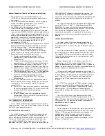
The Config_Enable signal (Pin 168) should be driven by
Altera FPGA logic similar to that shown in the following
VHDL process. Notice that after the Altera FPGA is
configured the Config_Enable signal is driven to a logic
low by the configured Altera FPGA. A logic low holds
the IP1K110 in user mode.
Process (Clock, Reset)
Begin
If (Reset = ‘1’) Then
Config_Enable <= ‘0’;
Elsif (Clock’event and Clock = ‘1’) Then
If (Write_Enable = ‘1’) Then
Config_Enable <= IP_Bus_D0;
Else
Config_Enable <= Config_Enable;
End If;
End If;
End Process
3.
The Config_Enable signal (Pin 168) can be driven to a
logic high via an IP bus write cycle to carrier base
a 0 hex with Data line 0 set high. Setting
Config_Enable high returns the IP1K110 to configuration
mode.
4.
After the Altera FPGA has returned control back to
configuration mode, the Altera FPGA must also: a)
disable drive of the IP bus Ack
∗
signal, b) disable drive
of the 16 IP bus data lines, and c) and disable IP bus
write cycles on the Altera FPGA. The following VHDL
code serves as an example of these requirements.
Process (ACK, Config_Enable)
Begin
If (Config_Enable = ‘0’) Then
ACK_n <= not ACK;
Else
ACK_n <= ‘Z’;
End If;
End Process
RD_Enable <= not Config_Enable and IO_Enable;
Process (RD_Data, RD_Enable)
Begin
If (RD_Enable = ‘1’) Then
IP_Data <= RD_Data;
Else
IP_Data <= (others => ‘Z’);
End If;
End Process
Write_Strobe <= MEMSEL_n and INTSEL_n and IDSEL_n and
not IOSEL_n and not RD_Write_n and not BSO_n and not
Config_Enable;
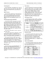
IP Identification Space (Read Only, 32 odd-byte addresses)
Each IP module contains identification (ID) information that
resides in the ID space per the IP module specification. This
area of memory contains 32 bytes of information at most. Both
fixed and variable information may be present within the ID
space. Fixed information includes the "IPAH" identifier, model
number, and manufacturer's identification codes. Variable
information includes unique information required for the module.
The IP1K110 ID space does not contain any variable (e.g. unique
calibration) information. ID space bytes are addressed using only
the odd addresses in a 64 byte block (on the “Big Endian”
VMEbus). Even addresses are used on the “Little Endian” PC
ISA or PCI buses.
The IP1K110 ID space will read differently in configuration
mode than it does in user mode. In configuration mode the IP
model code at base a 0Bhex will read a 42hex, while in
user mode the same byte will read 43hex. In addition, the CRC
byte at base a 17hex will read a 4Fhex in configuration
mode and read a 2Ehex in user mode. All other ID space bytes
will read the same in both configuration mode and user mode.
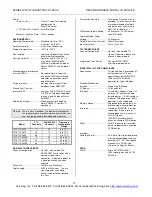
The example Altera FPGA file provided with the IP1K110
EDK implements the ID Space as shown in Table 3.2. Note that
the base-address for the IP module ID space (see your carrier
board instructions) must be added to the addresses shown to
properly access the ID information. Execution of an ID Space
Read operation requires 0 wait states.
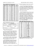
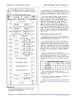
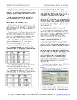
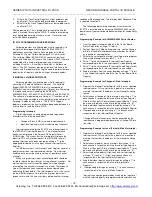
Table 3.2: IP1K110 ID Space Identification (ID)
Hex Offset
From ID
Base
Address
ASCII
Character
Equivalent
Numeric
Value
(Hex)
Field
Description
01
I
49
All 32MHz IP's
have 'IPAH'
03
P
50
05
A
41
07
H
48
09
A3
Acromag ID Code
0B
42
43
IP Model Code
1
42 = Config.
Mode
43= User Mode
0D
00
Not Used
(Revision)
0F
00
Reserved
11
00
Not Used (Driver
ID Low Byte)
13
00
Not Used (Driver
ID High Byte)
15
0C
Total Number of
ID PROM Bytes
17
4F
2E
CRC
4F= Config. Mode
2E= User Mode
19 to 3F
yy
Not Used
Notes (Table 3.2):
1. The IP model number is represented by a two-digit code
within the ID space (the IP1K110 model is represented by 42
Hex when in configuration mode and 43 Hex in user mode).
Example Altera FPGA Design
The example design provided with the IP1K110 EDK consists
of IP bus interface logic, Altera interface to 64K x 16 static RAM,
Altera interface to clock generator chip, and I/O interface to
differential or TTL I/O.
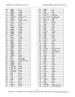
The IP1K110 hardware supports a direct connection to all IP
bus signals as listed in Table 2.2. As such, hardware will support
all IP bus cycles including: ID, I/O, Interrupt, Memory, and DMA.
The example design provided uses all but the Memory and DMA
cycle types.


