background image

SERIES IP503 INDUSTRIAL I/O PACK                  EIA/TIA-232E & CENTRONICS COMMUNICATION MODULE
___________________________________________________________________________________________

- 11 -

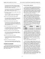
Line Status Register  continued

LSR Bit

FUNCTION

PROGRAMMING

2

Parity Error
(PE)

0 = No Error
1 = Parity Error - the received
character does not have the correct
parity as configured via LCR bits 3
& 4This bit is set high on detection
of a parity error and reset low when
the host CPU reads the contents of
the LSR.  In the FIFO mode, the
parity error is associated with a
particular character in the FIFO
(LSR Bit 2 reflects the error when
the character is at the top of the
FIFO)

3

Framing
Error (FE)

0 = No Error
1 = Framing Error - Indicates that
the
received character does not have
a valid stop bit (stop bit following
last data bit or parity bit detected
as a zero/space bit)This bit is
reset low when the CPU reads the
contents of the LSR.  In FIFO
Mode, the framing error is
associated with a particular
character in the FIFO (LSR Bit 3
reflects the error when the
character is at the top of the
FIFO)

4

Break
Interrupt (BI)

0 = No Break
1 = Break - the received data input
has been held in the space (logic 0)
state for more than a full-word
transmission time (start bits + data
+ parity bit + stop bits)Reset upon
read of LSR.  In FIFO mode, this bit
is associated with a particular
character in the FIFO and reflects
the Break Interrupt when the break
character is at the top of the FIFO.
It is detected by the host CPU
during the first LSR read.  Only one
“0” character is loaded into the FIFO
when BI occurs

5

Transmitter
Holding
Register
Empty
(THRE)

0 = Not Empty
1 = Empty - indicates that the
channel is ready to accept a new
character for transmission.  Set high
when the character is transferred
from the THR into the transmitter
shift register
Reset low by loading the THR
(It is not reset by a host CPU
read of the LSR)In FIFO
mode, this bit is set when the
Tx FIFO is empty and cleared
when one byte is written to the
Tx FIFO.  When a Transmitter
Holding Register Empty
interrupt is enabled by IER bit
1, this signal causes a priority 3
interrupt in the IIR.  If the IIR
indicates that this signal is
causing the interrupt, the
interrupt is cleared by a read of
the IIR

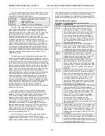
Line Status Register  continued

LSR Bit

FUNCTION

PROGRAMMING

6

Transmitter
Empty (TEMT)

0 = Not Empty
1 = Transmitter Empty - set when
both the Transmitter Holding
Register (THR) and the
Transmitter Shift Register
(TSR) are both empty.  Reset
low when a character is loaded
into the THR and remains low
until the character is
transmitted (it is not reset low
by a read of the LSR)In FIFO
mode, this bit is set when both
the transmitter FIFO and shift
register are empty

7

Receiver FIFO
Error

0 = No Error in FIFO (always 0 in
16C450 mode--FCR bit 0 low)
1 = Error in FIFO - set when one
of
the following data errors is
present in the FIFO: parity
error, framing error, or break
interrupt indication.  Cleared by
a host CPU read of the LSR if
there are no subsequent errors
in the FIFO

Note that LSR Bits 1-4 (OE, PE, FE, BI) are the error

conditions that produce a receiver-line-status interrupt (a priority 1
interrupt in the IIR register when any one of these conditions are
detected)This interrupt is enabled by setting IER bit 2 to 1

For the LSR & MSR registers, the setting of the status bits

during a status register read operation is inhibited (the status bit
will not be set until the trailing edge of the read)However, if the
same status condition occurs during a read operation, that status
bit is cleared on the trailing edge of the read instead of being set
again

A power-up or system reset sets all LSR bits to 0, except bits

5 and 6 which are high

MSR - Modem Status Register, Ports A & B (Read/Write)

The Modem Status Register (MSR) provides the host CPU

with an indication on the status of the modem input lines from a
modem or other peripheral device.  This register allows the
current state of the four modem input lines (CTS, DSR, RI, and
DCD) to be read (bits 4-7) and provides indication on whether the
states of these lines have changed since the last read of the
MSR (bits 0-3 are set high when the corresponding control inputs
from the modem changes state and are reset low when the CPU
reads the MSR)

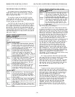
MSR - Modem Status Register

MSR BIT

FUNCTION

0

CTS (Set if CTS has changed states since last

read of MSR)

1

DSR (Set if DSR has changed states since last

read of MSR)

2

RI (Trailing Edge Only - Indicates RI* input to the

serial channel has changed state from Low-to-High
since last read of MSR)Not affected by High-to-Low
RI* transitions

3

DCD (Set if DCD has changed states since last

read of MSR)

Summary of Contents for Series IP503

Page 1: ...tion Module USER S MANUAL ACROMAG INCORPORATED 30765 South Wixom Road P O BOX 437 Wixom MI 48393 7037 U S A Tel 248 624 1541 Fax 248 624 9234 Copyright 1995 Acromag Inc Printed in the USA Data and spe...

Page 2: ...toring system This is especially important where economic property loss or human life is involved It is important that the user employ satisfactory overall system design It is agreed between the Buyer...

Page 3: ...m performance with precision analog I O applications The X suffix of the model number denotes the length in feet Model 5029 944 IP503 Serial Communication Cable A 5 foot long flat 50 pin cable with a...

Page 4: ...n assignments are unique to each IP model see Table 21 and normally correspond to the pin numbers of the field I O interface connector on the carrier board you should verify this for your carrier boar...

Page 5: ...ground to safety ground via any device connected to these ports or a ground loop will be produced and this may adversely affect operation The communication cabling of the P2 interface carries digital...

Page 6: ...ing Little Endian uses even byte addresses to store the low order byte As such use of this module on an ISAbus PC AT carrier board will require the use of the even address locations to access the 8 bi...

Page 7: ...transmitted then data is right justified to the LSB If parity is used then LCR bit 3 parity enable and LCR bit 4 type of parity are required Status for the receiver is provided via the Line Status Reg...

Page 8: ...gh to low transition start bit When the start bit is detected a counter is reset and counts the 16x sampling clock to 7 1 2 which is the center of the start bit The receiver then counts from 0 to 15 t...

Page 9: ...NOT supported by this model FIFO Control Register FCR BIT FUNCTION 0 When set to 1 this bit enables both the Tx and Rx FIFO s All bytes in both FIFO s can be cleared by resetting this bit to 0Data is...

Page 10: ...m Control Register 1 MCR Bit 4 provides a local loopback feature for diagnostic testing of the UART channel When set high the UART serial output connected to the TXD driver is set to the marking logic...

Page 11: ...d by a read of the IIR Line Status Register continued LSR Bit FUNCTION PROGRAMMING 6 Transmitter Empty TEMT 0 Not Empty 1 Transmitter Empty set when both the Transmitter Holding Register THR and the T...

Page 12: ...data lines This register is either output only or bi directional depending on the state of the extended mode bit bit 0 of the LEM register and the data direction control bit bit 5 of the LPC register...

Page 13: ...interrupt source the ACKN line of the parallel port or bit 2 of the LPS register The serial ports and the parallel port interrupts drive INTREQ0 Bit 0 of this register drives the ENIRQ line of the UA...

Page 14: ...atus of each channel can be read by the host CPU at any time during operation Two registers are used to report the status of a serial channel the Line Status Register LSR and the Modem Status Register...

Page 15: ...s the last stop bit time when the following occurs Bit 5 of the LSR THRE is 1 and there is not a minimum of two bytes at the same time in the transmit FIFO since the last time THRE 1The first transmit...

Page 16: ...Divisor Latch Access bit to permit access to the two divisor latch bytes used to set the baud rate These bytes share addresses with the Receive and Transmit buffers and the Interrupt Enable Register...

Page 17: ...puters are considered DTE devices while modems are DCE devices The EIA TIA 232E interface is the fifth revision of this standard and defines an unbalanced single ended transmission standard for unidir...

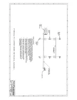
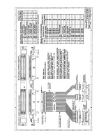
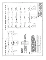
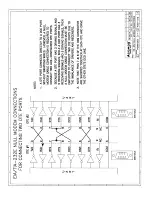
Page 18: ...ver a null modem cable connection is required to connect two like configured DTE ports due to the imbalance of drivers and receivers see Drawing 4501 572 Pins 1 18 of field I O connector P2 provide co...

Page 19: ...S INPUT BUSY Pin 11 Input Line Printer Busy Active high signal from the printer that is asserted when the printer is not ready to accept more Data The state of this bit is monitored via Bit 7 of the L...

Page 20: ...o obtain parts and repair PRELIMINARY SERVICE PROCEDURE Before beginning repair be sure that all of the procedures in Section 2 Preparation For Use have been followed Also refer to the documentation o...

Page 21: ...t maximum Choose shielded or unshielded cable according to model number The unshielded cable is recommended for digital I O while the shielded cable is recommended for optimum performance with precisi...

Page 22: ...Boards Application This panel converts the high density ribbon cable connectors coming from the APC8600 carrier board Acromag cable Model 5029 900 to screw terminals for direct wired interfaces This p...

Page 23: ......

Page 24: ......

Page 25: ......

Page 26: ......

Page 27: ......

Page 28: ......

Page 29: ......

Page 30: ......

Page 31: ......

Reviews: