Copyright © Siemens AG 2010. All rights reserved.
Page
56
ERTEC 400 Manual
Technical data subject to change
Version 1.2.2
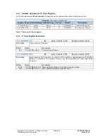
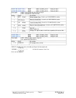
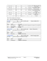
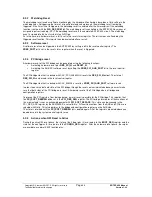
SSPIIR/SSPICR
R/W
Addr.: 0x4000_2214 Default: 0x0000
Description
SPI interrupt identification register (read)
SPI interrupt clear register (write)
Bit No.
Name
Description
0
RIS (Read)
SPI Receive FIFO service request interrupt status
0 = SSPRXINTR is not active
1 = SSPRXINTR is active
1
TIS (Read)
SPI Transmit FIFO service request interrupt status
0 = SSPTXINTR is not active
1 = SSPTXINTR is active
2
RORIS (Read)
SPI Receive FIFO overrun interrupt status
0 = SSPRORINTR is not active
1 = SSPRORINTR is active
15-3
---------- (Read)
Read: Reserved - value is undefined
15-0
---------- (Write)
Write: Receive overrun interrupt is deleted without check to determine
whether data are currently being written.
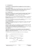
4.8 System Control Register
The system control registers are ERTEC 400-specific control registers that can be read and written to from the
PCI/LBU side or from the ARM946. A listing of all system control registers and their address assignments as well
as a detailed description are included in the following sections.
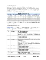
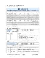
4.8.1
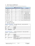
Address Assignment of System Control Registers
The system control registers are
32 bits in width
.
System Control Registers
(Base address 0x4000_2600)
Register Name
Offset Address
Address Area
Access
Default
Description
ID_REG
0x0000
4 bytes
R
0x40260100
ID ERTEC 400
BOOT_REG
0x0004
4 bytes
R
0x----
Boot mode pins Boot[0:2]
CONFIG_REG
0x0008
4 bytes
R
0x----
ERTEC 400 config pins
Config[0:4]
RES_CTRL_REG
0x000C
4 bytes
W/R
0x00000100
Control register for reset of
ERTEC 400
RES_STAT_REG
0x0010
4 bytes
R
0x00000004
Status register for reset of
ERTEC 400
PLL_STAT_REG
0x0014
4 bytes
R/W
0x00070005
Status register for PLL/FIQ3
CLK_CTRL_REG
0x0018
4 bytes
W/R
0x00000001
Control register for clock of
ERTEC 400
PM_STATE_REQ_REG
0x001C
4 bytes
R
0x00000000
Required power state of the PCI
host
PM_STATE_ACK_REG
0x0020
4 bytes
R/W
0x00000000
Current power state of ERTEC 400
PME_REG
0x0024
4 bytes
R/W
0x00000000
Power management event PME
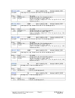
QVZ_AHB_ADR
0x0028
4 bytes
R
0x00000000
Address of incorrect addressing on
multilayer AHB
QVZ_AHB_CTRL
0x002C
4 bytes
R
0x00000000
Control signals of incorrect
addressing on multilayer AHB
QVZ_AHB_M
0x0030
4 bytes
R
0x00000000
Master detection of incorrect
addressing on multilayer AHB
QVZ_APB_ADR
0x0034
4 bytes
R
0x00000000
Address of incorrect addressing on
AHB
QVZ_EMIF_ADR
0x0038
4 bytes
R
0x00000000
Address that leads to timeout on
EMIF
PCI_RES_REQ
0x003C
4 bytes
R/W
0xFFFF0002
Request register for placing a SW
reset request on the PCI bridge

