Copyright © Siemens AG 2010. All rights reserved.
Page
71
ERTEC 400 Manual
Technical data subject to change
Version 1.2.2
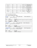
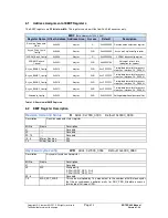
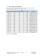
SDRAM Bank Config
W/R
Addr.: 0x7000_0008 Default: 0x0000_20A0
Description
SDRAM bank config register
Bit No.
Name
Description
31..15
----
Reserved
14
WB
Write burst type
0: Programmed burst length
1: Single write (not permitted for 16-bit SDRAM bank)
13*
CL
CAS latency
0: SDRAM is activated with CAS latency = 2
1: SDRAM is activated with CAS latency = 3
12..11
----
Reserved
10..8*
ROWS
000: 8-row address lines
001: 9-row address lines
010: 10-row address lines
011: 11-row address lines
100: 12-row address lines
101: 13-row address lines
110: 14-row address lines
111: 15-row address lines
7
----
Reserved
6..4
IBANK
Internal SDRAM bank setup (number of banks in the SDRAM)
000: 1 bank
001: 2 banks
010: 4 banks
011 .. 111: Reserved
3
----
Reserved
2..0
PAGESIZE
Page size
000: SDRAM with 8-column address lines
001: SDRAM with 9-column address lines
010: SDRAM with 10-column address lines
011: SDRAM with 11-column address lines
100..111: Reserved
*) Attention: Writing to SDRAM_Bank_Config executes the Mode Register Set command on the SDRAM if Bit 29
(init_done) is set in the SDRAM_Refresh_Control register (i.e., the SDRAM power-up sequence has been
executed).
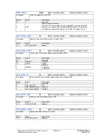
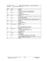
SDRAM Refresh Control
W/R
Addr.: 0x7000_000C Default: 0x0000_0190
Description
Setting of refresh rate, indication for timeout
Bit No.
Name
Description
31
----
Reserved
30
AT
(Read only)
Asynchronous timeout
Set to 1 in event of timeout
29
INIT_DONE
(Read only)
SDRAM initialization done
0: SDRAM power-up sequence is running
1: SDRAM power-up sequence is complete
28..13
----
Reserved
12..0
REFRESH_RATE
Refresh rate
Number of AHB clock cycles between 2 SDRAM refresh cycles

