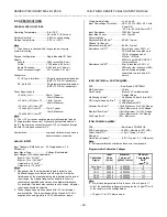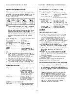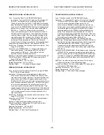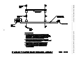
SERIES IP330 INDUSTRIAL I/O PACK 16-BIT HIGH DENSITY ANALOG INPUT MODULE
___________________________________________________________________________________________
- 8 -
in the Motorola 68000 microprocessor family and is the VMEbus
convention. In Big Endian, the lower-order byte is stored at odd-
byte addresses. The Intel x86 family of microprocessors uses the
opposite convention, or “Little Endian” byte ordering. Little Endian
uses even-byte addresses to store the low-order byte. As such,
installation of this module on a PC carrier board will require the
use of the even address locations to access the lower 8-bit data
while on a VMEbus carrier use of odd address locations are
required to access the lower 8-bit data.
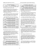
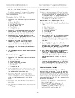
Control Register, (Read/Write) - (Base + 00H)
This read/write register is used to: select the output data
format, select the external trigger signal as an input or output,
select acquisition input mode, select scan mode, enable/disable
the timer, and select the interrupt mode.
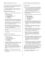
The function of each of the control register bits are described
in Table 3.3. This register can be read or written with either 8-bit
or 16-bit data transfers. A power-up or system reset sets all
control register bits to 0.
Table 3.3: Control Register
BIT FUNCTION
0 Not
Used
1
1
Output Data Format
0 = Binary Two’s Complement
1 = Straight Binary
See Tables 3.4 and 3.5 for a description of these
two data formats.
2 External
Trigger
0 = Input
1 = Output
It is possible to synchronize the data acquisition of
multiple IP330 modules. A single master IP330
module must be selected to output the external
trigger signal while all other IP330 modules are
selected to input the external trigger signal. The
external trigger signal (pin 49 of the field I/O
connector) must also be wired together.
5,4,3
Acquisition Input Mode
000 = All Channels Differential Input
001 = All Channels Single Ended Input
010 = Not Used
011 = 4.9000v Calibration Voltage Input
100 = 2.4500v Calibration Voltage Input
101 = 1.2250v Calibration Voltage Input
110 = 0.6125v Calibration Voltage Input
111 = Auto Zero Calibration Voltage Input
7,6 Not
Used
1
10,9,8 Scan
Mode
000 = Disable
001 = Uniform Continuous
010 = Uniform Single
011 = Burst Continuous
100 = Burst Single
101 = Convert on External Trigger Only
110 = Not Used
111 = Not Used
See the Modes of Operation section for a
description of each of these scan modes.
11 Timer
Enable
0 = Disable
1 = Enable
BIT FUNCTION
13,12 Interrupt
Control
00 = Disable Interrupts
01 = Interrupt After Convert of Each Channel
10 = Interrupt After Conversion of all selected
channels is completed. A group of channels
includes all channels from the Start Channel up
to and including the End Channel value.
11 = Disable Interrupts
14,15 Not
Used
1
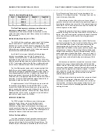
Notes (Table 3.3):
1. All bits labeled “Not Used” will return on a read access the last
value written.
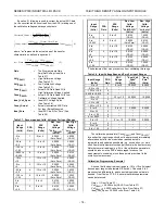
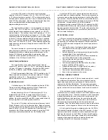
Analog Input Ranges and Corresponding Digital Output Code
Selection of an analog input range is implemented via the DIP
switch setting given in Table 2.1. The ideal input voltage
corresponding to each of the supported input ranges is given in
Table 3.4. Then in Table 3.5 the digital output code corresponding
to each of the given ideal analog input values is given in both
binary two’s complement and straight binary formats.
Table 3.4: Supported Full-Scale Ranges and Ideal Analog Input
DESCRIPTION
ANALOG INPUT
Input Range
±
10V
0 to 10V
±
5V
0 to 5V
LSB (Least
Significant Bit)
Weight
305
µ
V 153
µ
V 153
µ
V 76
µ
V
+ Full Scale
Minus One LSB
9.999695
Volts
9.999847
Volts
4.999847
Volts
4.999924
Volts
Midscale
0V 5V 0V 2.5V
One LSB Below
Midscale
-305
µ
V
4.999847
Volts
-153
µ
V
2.499924
Volts
- Full Scale
-10V 0V -5V 0V
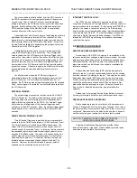
The digital output format is controlled by bit-1 of the Control
register. The two formats supported are Binary Two’s
Complement and Straight Binary. The hex codes corresponding to
these two data formats are depicted in Table 3.5.
Table 3.5: Digital Output Codes and Input Voltages
DIGITAL OUTPUT
Binary 2’s Comp
Straight Binary
DESCRIPTION
(Hex
Code)
(Hex Code)
+ Full Scale - 1 LSB
7FFF
FFFF
Midscale 0000
8000
1 LSB Below Midscale
FFFF
7FFF
- Full Scale
8000
0000
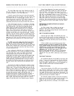
Interrupt Vector Register (Read/Write, 03H)
The Vector Register can be written with an 8-bit interrupt
vector. This vector is provided to the carrier and system bus upon
an active INTSEL* cycle. Read or writing to this register is
possible via 16-bit or 8-bit data transfers. 16-bit data transfers will
implement simultaneous access the Interrupt Vector and Timer
Prescaler registers. The register contents are cleared upon reset.

