SERIES IP330 INDUSTRIAL I/O PACK 16-BIT HIGH DENSITY ANALOG INPUT MODULE
___________________________________________________________________________________________
- 14 -
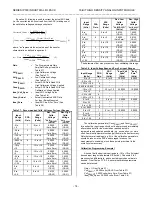
Equation (1) following is used to correct the actual ADC data
(i.e. the uncorrected bit count read from the ADC) making use of
the calibration voltages and range constants.
Corrected_ Count =
65536
m
Ideal_ Volt_ Span
∗
*
Count_
(VoltCALLO *Gain)- Ideal_ Zero
m
CountCALLO (1)
−
where, "
m
" represents the actual slope of the transfer
characteristic as defined in equation 2:
m = Gain
VoltCALHI VoltCALLO
CountCALHI CountCALLO
(2)
∗
−
−
Gain
=
The Programmable Gain
Amplifier Setting Used (See
Table 3.7)
VoltCALHI
=
High Calibration Voltage
(See Table 3.7)
VoltCALLO
=
Low Calibration Voltage
(See Table 3.7)
CountCALHI
=
Actual ADC Data Read With
High Calibration Voltage Applied
CountCALLO
=
Actual ADC Data Read With Low
Calibration Voltage Applied
Ideal_Volt_Span
=
Ideal ADC Voltage Span
(See Table 3.8)
Count_Actual
=
Actual Uncorrected ADC Data
For Input Being Measured
Ideal_Zero
=
Ideal ADC Input For “Zero” (See
Table 3.8)
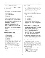
Table 3.7: Recommended Calib. Voltages For Input Ranges
Input
Range
(Volts)
PGA
Gain
ADC
Range
(Volts)
Rec. Low
Calib.
Voltage
"VoltCALLO"
(Volts)
Rec. High
Calib.
Voltage
"VoltCALHI"
(Volts)
-5 to
+5
1
-5 to +5
0.0000
(Auto Zero)
4.9000
(CAL0)
-2.5 to
+2.5
2
-5 to +5
0.0000
(Auto Zero)
2.4500
(CAL1)
-1.25 to
+1.25
4
-5 to +5
0.0000
(Auto Zero)
1.2250
(CAL2)
-0.625 to
+0.625
8
-5 to +5
0.0000
(Auto Zero)
0.6125
(CAL3)
-10 to
+10
1
-10 to +10
0.0000
(Auto Zero)
4.9000
(CAL0)
-5 to
+5
2
-10 to +10
0.0000
(Auto Zero)
4.9000
(CAL0)
-2.5 to
+2.5
4
-10 to +10
0.0000
(Auto Zero)
2.4500
(CAL1)
-1.25 to
+1.25
8
10 to +10
0.0000
(Auto Zero)
1.2250
(CAL2)
0 to
+5
1
0 to +5
0.6125
(CAL3)
4.9000
(CAL0)
0 to
+2.5
2
0 to +5
0.6125
(CAL3)
2.4500
(CAL1)
Input
Range
(Volts)
PGA
Gain
ADC
Range
(Volts)
Rec. Low
Calib.
Voltage
"VoltCALLO"
(Volts)
Rec. High
Calib.
Voltage
"VoltCALHI"
(Volts)
0 to
+1.25
4
0 to +5
0.6125
(CAL3)
1.2250
(CAL2)
0 to
+0.625*
8
0 to +5
0.0000
(Auto Zero)*
0.6125
(CAL3)
0 to
+10
1
0 to +10
0.6125
(CAL3)
4.9000
(CAL0)
0 to
+5
2
0 to +10
0.6125
(CAL3)
4.9000
(CAL0)
0 to
+2.5
4
0 to +10
0.6125
(CAL3)
2.4500
(CAL1)
0 to
+1.25
8
0 to +10
0.6125
(CAL3)
1.2250
(CAL2)
*The hardware offset may prevent you from calibrating this range.
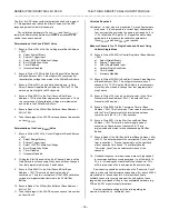
Table 3.8: Ideal Voltage Span and Zero For Input Ranges
Input Range
(Volts)
PGA
Gain
ADC
Range
(Volts)
"Ideal_Volt
_Span"
(Volts)
"Ideal_
Zero"
(Volts)
-5 to +5
1
-5 to +5
10.0000
-5.0000
-2.5 to +2.5
2
"
"
"
-1.25 to +1.25
4
"
"
"
-0.625 to +0.625
8
"
"
"
-10 to +10
1
-10 to +10
20.0000
-10.0000
-5 to +5
2
"
"
"
-2.5 to +2.5
4
"
"
"
-1.25 to +1.25
8
"
"
"
0 to +5
1
0 to +5
5.0000
0.0000
0 to +2.5
2
"
"
"
0 to +1.25
4
"
"
"
0 to +0.625
8
"
"
"
0 to +10
1
0 to +10
10.0000
0.0000
0 to +5
2
"
"
"
0 to +2.5
4
"
"
"
0 to +1.25
8
"
"
"
The calibration parameters (CountCALHI and CountCALLO)
for each active input range should not be determined immediately
after startup but after the module has reached a stable
temperature and updated periodically (e.g. once an hour, or more
often if ambient temperatures change) to obtain the best accuracy.
Note that several readings (e.g. 64) of the calibration parameters
should be taken via the ADC and averaged to reduce the
measurement uncertainty, since these points are critical to the
overall system accuracy.
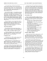
Calibration Programming Example 1
Assume that the desired input range is -10 to +10 volts (select
desired input range via hardware DIP switch). Channels 0 to 3
are connected differentially, and corrected input channel data is
desired. From Tables 3.7 & 3.8, several calibration parameters
can be determined:
Gain = 1 (From Table 3.7)
VoltCALHI = 4.9000 volts (CAL0; From Table 3.7)
VoltCALLO= 0.0000 volts (Auto Zero; From Table 3.7)
Ideal_Volt_Span = 20.0000 volts (From Table 3.8)

