13. JTAG > JTAG Register Access
111
PEB383 User Manual
July 25, 2011
Integrated Device Technology, Inc.
Confidential - NDA Required
13.6
JTAG Register Access
The JTAG Interface can be used for debug purposes in order to perform read and write access of the
PEB383’s configuration registers. It also can perform read accesses on the performance registers
without impacting active transactions.
A user-defined command enables the read and write capabilities of the JTAG Interface. This is in the
User Test Data Register (DR) set in the PEB383.
13.6.1
Register Access from JTAG
The format for access the PEB383’s DR register using JTAG is shown in the following figures. The
same DR register is used for read and write access.
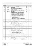
Figure 37: Read/Write Access from JTAG — Serial Data In
Figure 38: Observe from JTAG — Serial Data Out
13.6.2
Write Access to Registers from the JTAG Interface
Complete the following steps to write to a device register through the JTAG Interface:
1.
Move to the TAP controller “Shift-IR” state and program the instruction register with the
instruction of the DR by writing into Instruction Register bits with 0xFFFF_FFFF_FFFF_FFFD.
2.
Move to the “Shift-DR” state and shift the data[31:0], R/W = 1 and the address[9:0] serially in the
TDI pin. To prevent corruption of unused bits, the full DR bits have to be written as follows (see
also
•
DR[66:62] = 5b’0
•
DR[61:52] = ADDR[9:0]
1
•
DR[51] = R/W
•
DR[50:19] = DATA[31:0]
•
DR[18:17] = 2b’0
Ti
p
For more information about the test data register, see Test Technology Standards Committee:
IEEE Computer Society,
IEEE Standard Test Access Port and Boundary-Scan Architecture
,
IEEE Std. 1149.1-1990, 1149.1a-1993, October, 1993., Section 8.3.
1. Note that the address here is the DWORD address, not the byte address. Take the byte address and remove the 2 LSBs, >>2.
JTAG_TDI
JTAG_TDO
Address [9:0]
R/W
Ready
Error
Data [31:0]
Rsvd [16:0]
Reserved [66:62]
JTAG_TDI
JTAG_TDO
Data [31:0]
Error
Reserved [66:34]
Ready


